Micro G PIC Ultimate
To obtain a singleor
copy write to the PCB ad.noctis@gmail.com
while stocks last
Tutorial
available on the Internet for use and operation of the development:
-
Part one (only in. Doc). How to create the project, obtain the file. Hex and
test the operation of the simulator
-
Part
second Tutorial "link the card to the PC via
232
-
Part Three of the
Tutorial "use of 'I / O digital versatile Micro-GT PIC IDE
With I.D.E. is
mean Developed Integrated Environment then Cn development system
projects microcontrollers, the PIC series, capable of integrating a high
number of peripheral devices. The electronic card contains: A programmer
compatible serial 8076, housing for a 2x16 character LCD display,
the space for a graphic display Glcd (graphic liquid crystal display) 128
x 64 points, an H bridge from 8 amps continuous, a dual full bridge for the L298
drive a stepper motor bipolar or two DC motors to
up to 2 amps, a 7-segment LED display 4 digits in controllable
multiplexer providing BCD code to the integration of decoding, 16 buttons
jumper selectable pull up or pull down in groups of 4, 24 outputs
maximum indicated by digital LEDs, Streep direct access to I / O
PIC, 8 analog inputs with simulated trimmer. A large number of dip
selectable switches and jumpers allow you to change the functionality of
various points of connection to the PIC. It can easily connect a high
number of actuators. The system is designed to program the PIC
40, 28, 18-pin dual in line, and in other ways ICSP (in circuit serial
programming) and you can move the clock signal, or even
select an appropriate setting of quartz with a jumper with
jumpers.

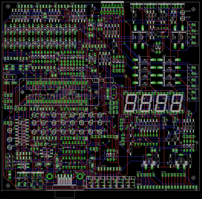
The support developed PCB
FR4 technology (dual layer) so far 164 mm x 156mm.
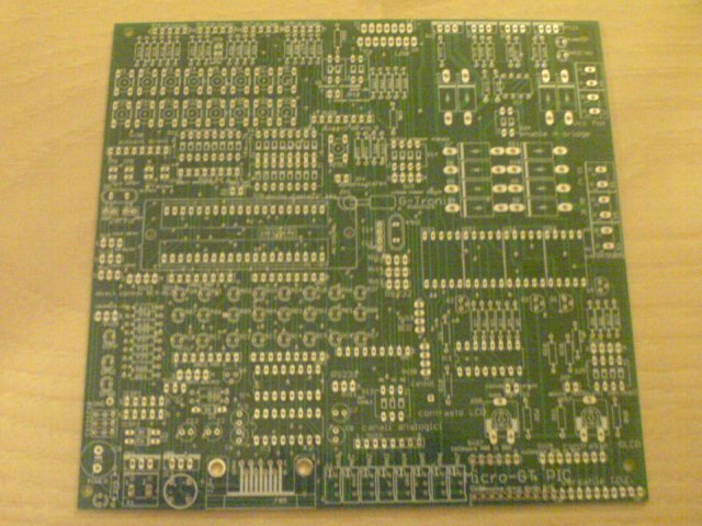
After
launch the automatic routing of the PCB looks like in the picture
below, we note that a single missing link fortunately
marginal interest between LED 11 and the jumper SV13. We will attempt to resolve
but the problem manually in case of failure must be carried by running
this link via a bridge wire wrap. The result is still very
satisfactory given the complexity of the circuit and the compact size. The
circuit is now optimized by increasing the slopes where possible. will indeed
a must to maximize the thicknesses of the zones used to control
power, ie insofar as it relates to the bridge chip and H
multiwatt L298 to drive a bipolar stepper motor.

Download the layout with the routing
In the next
image we see a copy of the PCB made.
Files
gerber construction can be found by contacting
bonzisandy88@hotmail.com that will help make you an interpreter
ordering at a Chinese factory.
Download PDF
Schematic
Download Schematic and PCB in Eagle
Format
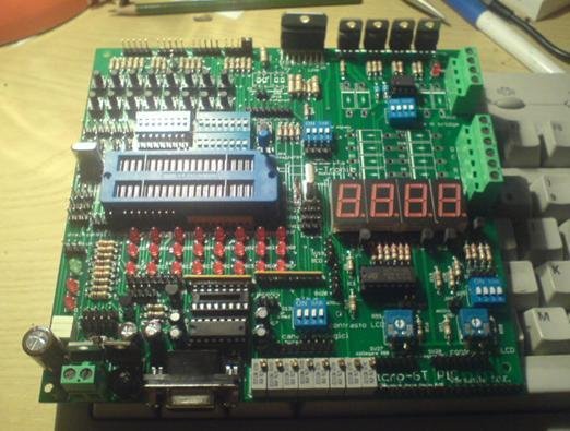
The underlying
picture we can see some examples of the PIC Micro-GT versatile IDE
to assembled from Internet users after you get the PCB.
Copy edited by Luca Luise, User www.grix.it. After have made this wonderful specimen, and be signed
extensive testing has offered to perform the fittings for the less
experts. To know how much it costs you a copy assembled and tested
get in touch with him ever passing through at
Email: ad.noctis@gmail.com
Copy performed by Matthew Pontarollo,
student of social and cultural center ZIP (industrial area of Padua
centrozip@libero.it) In a
editions of the basic course of programming PIC. The base is
PIC16F877A installed.
Power
Nourish
card at any voltage, either continuous or alternating current (entered a
bridge rectifier which provides a possible reversal) between
a minimum of 15V, since in some points must be 13.2 V for the flasche
PIC and must take account of the fall of drop-out of the LM stabilizers, and
a value of "ragionaevole" for the endurance of the same. It could be
example 18Va.c. or 24V dc, make sure that you alternate straightening the
multiply the nominal value of the transformer to the root of two,
or 1.4. In any case never exceed 30V, or about
value of the LM crash.
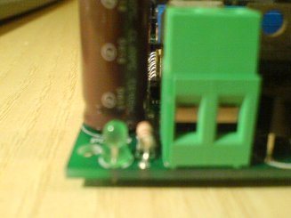
Position of the LED that indicates
power-system development Micro-GT
Communication
with the Micro Serial-GT PIC.
The serial communication
even programming with the Micro-GT is via the connector
DB9 female mounted on board. Though it would be better
connect through a real serial port of a desktop PC the link can
also occur via a USB-> RS232 interface for
with today's notebook that fitted more to this port
flasche the PIC using ICSP mode (in circuit serial programming)
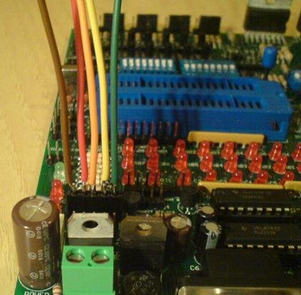
for which you need to build in a 5-wire connector, visible in the figure, for which there will be an advantage if
respect the same colors.

ICSP connector to be built
using 5 position streep female line (if possible meet the
colors).
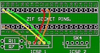
The correct position of
ICSP connector is shown in the next figure. you can use
either the connector ICSP1 or ICSP2 on board
tab, since these are parallel and may even
allow the programming of two chips at a time (to an external
tab). It is recommended, when they are rispettai the colors,
keep Brown on the right. The suggestion of the colors is
because it is not yet released the software
dedicated "MG-Lab, is taking care of it cu his friend Fabio,
provisionally PICPRO2009 we will use the (easily findable on the net)
that will recognize the device as "8076", or set as ICPROG
JDM reversed cable set (depends on the serial cable used).
ICSP connectors are
just above the voltage regulators.
Launching ICPROG 2009, and
entering the test section and communication, above right,
Power on, indicating it meets the correct position of
free end of the ICSP connector of the colored wires in question. maneuver
essential for programming the microcontroller. And 'good
Always keep the schemes in hand.
PICPROG 2009, during the
function tests suggests that pin to connect the wires that are colored
were used for the construction of the ICSP connector. These changes
every time you change the chip to be programmed.
ICSP settings
During the communication
and
the test using the flash
you will see PICPROG2009. Three LEDs on the side
of the ICSP connector, you'll immediately notice that the sequence
is not quite the same as
two LEDs will be reversed. Not worry about this,
remember that you are using a software
expedient, or a
provisional until it is ready
specific MG-Lab in which
the thing is already settled. However, this is only
of a signal bit in
transit (so no problem),

Signalling LED
the state of the bus for programming and communication.
The serial cable to be used
will type with two CANNON DB9 male connectors on the board side PIN
to PIN or a simple extension. Do not perform any intersection.
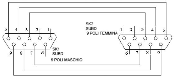
Wiring diagram for the cable
serial to use.
Studio Modular
project
Module
power at two levels
The module allows
power circuit with two voltage levels, a suitable
device programming PIC approximately 13.5 volts and a TTL (5V) for the
normal power of logic circuits. The voltage of 13.2 is obtained
exploiting the power generator on pin central regulators
uA78xx positive voltage range. On this leg there is a generator
4mA current that constantly pushes toward creating the standard for mass
the internal circuitry. By inserting two forward biased diodes between
center pin and the mass is added to the regulated voltage twice
Vgamma junction voltage = 0.6 volts. We get so much for the 13.2
switch in the pic programming. The PCB was added to a test point in
close dell'elettrolitico C9 which provides a ground.
discover developing their own projects how useful this point
access to the mass.

The lines that we see out of the positive
of
electrolytic C2 leads the voltage at the connector for programming
serial circuit (ICS1 and ICS2).
The voltage regulator IC3 is a
uA7805, and provides voltage to all the TTL logic circuit. The Power LED
indicates that the device is powered.
Important note: As it is
section was designed to power the circuit can be powered with
any voltage is alternating though between 9 and 36 times
volts which is the maximum limit of the regulator uA7812 we meet
first after the diodes.
The power supply section provides
about 1 amp more than enough for any state of development in
laboratory.
Input module
digital
The module
includes 16 push buttons on the type of mounting
PCB congener for both pressed into action to launch a 1
logical that a 0, depending on how they are configured by jumpers
related to streep SV1, SV2, SV3, SV4. Lining up all the jumpers in
buttons down the left launched a logical (in fact act as the resistance
by pull down while aligning the jumper on the right the same action
involves the launch of a logical zero (resistors act as pull up).

The inputs were dissected
in groups of 4 through steep SV1, SV2, SV3, SV4 so
to maximize the versatility of the circuit. You can simulate such a
multiples of 4 buttons is N.C. that N.A. on the machine, such as 4 N.C.
e12 NA It 's very useful function of insulation available
acting on the dip and dip S11 S12 (open switches). each button
If this continues to be nurtured and properly bound elle
TTL voltages (remains active configuration jumper on NO and NC), but now
we can bring through flat cables each of these signals at any point
or even outside of the circuit board after the board told
outside the same mass. The direct access to the buttons you can
connecting cables to the flat streep SV29 and SV30.
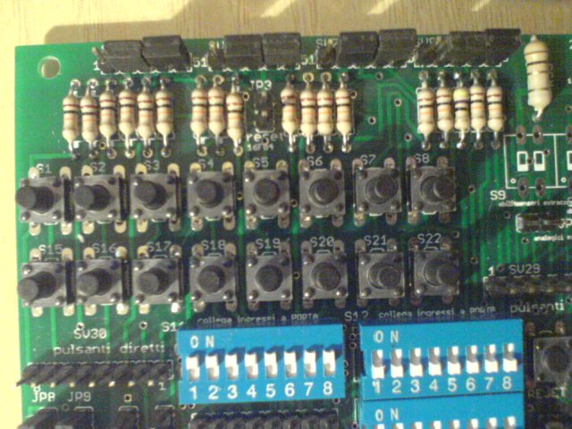
input section of the card
Micro-GT, are observed ipost pull-up jumpers, pull-down
Important note:
JP3 jumper must be closed when one is going to plan PIC 16F84
or a compatible 18-pin. The closure of JP3 involves connecting to ground
Pin 5 is essential for the device's power, obviously
this case the line should not be interrupted so the dip S11
must have the mandatory line 4-13 in the ON position. Required
in this case is also close the connector SV2 streep mode PULL UP
because only then will the lines to ground. Caution
polarity reversal of the feeding device even if the card
should prevent errors so gross as to be putting that Vss to Vdd
positive voltage or floating it does not result in the destruction
the CIP. S6 combines the function key to the case of MCLR or PIC16F84
microcontroller pin to pin compatible. If you wish to use this
function you need to configure the radio group S5, S6, S7, S8 must
with pull-up resistor (jumper flush right on the second group). If
you do not have this foresight program in the PIC will not start because
it receives
constantly reset signal.
Output Module
digital
The module
includes 24 digital outputs TTL logic level, which has been shown
by turning on an LED. Each of the three bytes of output can be excluded by means
1,2,3 dip switches on the S13 with the correspondence:
S13
1 -> PORT D
S13
2 -> C PORT
S13 3 ->
PORT D

It can be accessed directly
the PORT B PORT C PORT D, connected directly to SV18 streep (PORT
D), SV22 and SV23 (PORT C) and SV17 (PORT B). In the case of
direct access to the Port is not recommended to load the output
microcontroller with currents greater than a few tens of milliamps, use a
of these outputs to directly drive the coil of a relay would be really
a beginner's mistake that leads to damage to the device. Yes
also points out that for reasons of circuit simplicity has not been provided
for any input / output opto-isolation, on the other hand, this is a system
development and not a PLC although laboratory tests they can take the place.
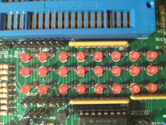
Digital output modules, each LED is
indicated by the silkscreen on the 40 pin versionIn
yellow resistance network.
Micro-GT PIC
base model
For a user
beginner to the complete assembly of the Micro-GT could be a load
Economic a little annoying but not impossible. While waiting for the
technical expertise to use all the modules in the layout you can
restriction to assembly of the bulk of the digital I / O. The board
takes the form shown in the picture:

Features
techniques are still very respectable when compared with many products
trade. The basic model shown in the figure shows:
-
8 inputs
Digital configurable jumper in groups of 4 pull-up or pull-down.
-
Free Port Mode
which allows for example to isolate the inputs and connect them to a port
different.
-
8 digital outputs,
isolated if you want to convert the output to PORTB inputs (figure I
put a jumper but deep enough to fit the expected 2-way).
-
1 serial port
232 switch from planning to supervision arrangements
(When a software controls the I / O such as servo motors)
-
two connectors
ICSP (in circuit serial programming)
-
1 to 20 MHz quartz
-
Unit
Dual voltage power supply (running at +5 V and +13.2 V programming)
-
1 socket textool
40 pin.
-
All PIC
flaschabili executables and the full version will remain so even in
basic version (of course).
We note the
ICSP cable position, the brown is the first left, while the
Red can be disconnected because there is redundancy in the PCB for that
wire.
Fix bug MCLR for use as a base model
When you plan to
use the PIC Micro-GT are the versatile IDE 28-pin PIC or 40 as the pin
16F876 or the 16F877, or their equivalent 18 series, can be dispensed with
under special conditions of use which the board can provide when
PIC installed are of use in reality rather rare. For a more
Quick connector ICSP eseguimo na small changes that consists of:
-
Cutting the track
that connects the reset button to pin 1
-
remove the solder
a few millimeters from the track
-
bending the pins
a lower line streep two positions so that we can support from
na part of the pitch reset button and the other to the copper track
cut we found scraping the tip of the cutter.
-
Weld the streep
line in this position, insert a jumper and check the meter if
reset by pressing the buzzer sounds between pin 1 of the processor and the mass, or
the heat sink controller 7805 (note: do not try with the 7812
because it is not grounded because of the two diodes in series on the center pin).
This
simple modification is documented in the following photos:

Cutting the track.
The conductor is cut at the Vias (hole metallic) of the track
next. As we can see the solder was removed gently scraping
the track surface with a knife. This maneuver should be done to give a little
of attention even if the card is not really so delicate that it threatens
functionality.

Solder the new two-streep
positions in place so that we have made. the picture is almost
paying attention to the invisible but we can see, is parallel to
el deepswitch the left edge, as close to the base textool.

Mode implementation of the
program jumper streep sneak in line at two positions, in the photo
we see him in blue. I chose this color to highlight its presence.

In programming mode, Streep just sneak it in one of two pins of the line streep (to be
the right) and in the left hand sneak the brown wire
ICSP connector, or its pin 1. This amendment resolves any
conflict of tensions that may arise between the Implementing Rules and
the programming modeornand pic of
40 and 28 pin.
We see a turn
demo 16F877A processor, it is of the classic supercar,
remember to line up the line streep SV13 and SV14 right, this
disable quartz 4Mhz passing the bus to the pins connected to the LED, or RB5
RB4 and how we can easily see with the patterns in the hand.
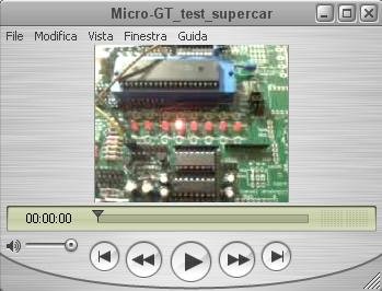
download movie dl
test "supercar to PORTB" Micro-GT PIC versatile IDE
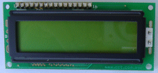
2x16 LCD Module characters
The module allows the management of a common
LCD type HD44780 compatible module, interfaced with the 4-bit method.
It will show any warning messages, or show data or
still bring the temperature detected by a sensor.
It can use two different models that differ from the display
otherwise the PIN.
The Micro-GT
versatile I.D.E. presents only the housing and PIN to link the
display using one or more flat cables, to avoid the waste of resources because
the use of the LCD is one of many possible features.

The jumper JP6
allows the backlight or power
anode-cathode of the LED integrated (PIN 15 16 anodoe cathode side display), while
streep the 3-terminal SV25 enables the connection of the first flat cable
three terminals of the LCD and is the 5 volt power supply and regulation
contrast.
With regard to
three lines needed to monitor RS / RW / E was added to the connector
SV4 three terminals. coinciding with the PIC 16F877A PORT D.
Warning: A ZIF socket
40 pin 3M is on ebay $ 0.99, equal to € 0.75, do not be fooled!
Buy on ebay even if you have to wait 10 days. Shipping included, there
costs less than 5 €.
The data lines
however, will be taken in one of the "direct access" to the port with
the freedom to decide (depending on the software developed for the PIC) the
mode 4 or 8 bits.
download the technical documentation of the display
In some models
the row of pins is shown (in parallel), even on the underside of support
Display PCB. Connecting to the one above or below it makes no difference, we use
therefore the most convenient for the wiring.
Description
The crystal display
liquid or LCD (Liquid Crystal Display English)
connected to This form has 2 lines of 16 characters
each. The LCD displays the most common commercially available, have
interface designed by Hitachi that, over time, has become a standard
Industrial also used by other manufacturers.
|
Function of various pins of the display
|
|
PIN |
Name |
Function |
|
1 |
GND |
Ground -
Pin must be connected to the negative supply. |
|
2 |
VDD |
Power Supply -
Pin to be connected to +5 V supply. |
|
3 |
Vo |
To this pin should enjoy a
variable voltage from 0 to +5 V through a trimmer to adjust the display contrast.
|
|
4 |
RS |
Register Select -
This pin is a line with which it communicates to the display
if
you are sending on the data bus (lines DB0 to DB7) a command (RS = 0)
or a data
(RS = 1). |
|
5 |
R / W |
Read, Write -
This pin is another line with which it communicates to
if you send a display means to display data (R / W = 0) or read
a display given by (R / W = 1).
|
|
6 |
E |
Enable -
This pin is a control line which can enable
display and accept data and instructions from the data bus (E = 1).
|
|
7 |
DB0 |
Data bus line 0 -
The lines to pass data between the processor and display. |
|
8 |
DB1 |
Data Bus Line 1 |
|
9 |
DB2 |
Data Bus Line 2 |
|
10 |
DB3 |
Data Bus Line 3 |
|
11 |
DB4 |
Data Bus Line 4 |
|
12 |
DB5 |
Data Bus Line 5 |
|
13 |
DB6 |
Data Bus Line 6 |
|
14 |
DB7 |
Data Bus Line 7 |
|
15 |
A |
Pin for connecting the
backlight if any.
|
|
16 |
K |
Pin for connecting the backlight if any.
|
Of the 16 pins if they use
However, only 7
RS Register select signal
E Enable signal
R / W read / wrwite selection
DB4 Data bit 4
DB5 Data bit 5
DB6 Data bit 6
DB7 Data bit 7
The data lines, RS and E
not are
with eveand a pull-down resistor to ground to force the line when
used. This was intended to maintain the
compatibility with other applications such as digital I / O pin in the same. In most cases the system will work, but if
need to add the three pulldown resistors there will be
big problems to install the outside, or edge of the display. You can
even use it in combination with SV16 line streep SV6 (see
schema) to connect the three resistors then closed to the more
near earth point.
The trimmer R55 connected to pin Vo,
through the line streep SV25 To adjust the contrast of the LCD.
Module 7-segment display, 4 digit
The module allows the management of 4
digit common cathode mode multiplexer controllable, ie it will be necessary
with the processor generating a BCD Nibble on the data bus and enabling the digit
corresponding with the launch of a Bit on the bases of transistors BC337
used in saturation, which will ban the lighting of the digit
correspondent.

particularly the seven-segment display and driver
CD4511, also highlighted the deep switch cutting and 4 for BJT
multiplex digit.
Warning: The PCB has the
sequence from left to right dis3, dis2, dis1, dis4 for reasons of convenience
routing.

download the documentation of the integrated CD4511
The IC CD4511 (equivalent to the TTL
74LS48 and LS248) takes care of the decoding of the four-bit
BCD generated with the PIC. If we use the on-board connections, which enabled
BUS using the dip switches S26 and in the case of a PIC16F877, you have the
correspondence:
A -> RB7
B -> RB6
C -> RB5
D -> RB4
As you can see from this diagram
signals are never floating even if the opening of the dip is 26
in fact brought to zero by the pulldown resistors.
Decimal points can be
separately controlled or isolated by the dip 25. If we wanted to
example, create a digital clock should only enable the dip 25
line number 2.
A good programming exercise
would be to modify the software presented on this site
on
clock 24 hours in order to do so
run on the PIC Micro-GT.
controls are: SV19 ->
direct entry of BCD data, SV20 -> control of the multiplexer
display (common cathode enables the driving transistor), SV21-> Control
4 decimal points on the display (isolated DIP 4 line S25.
Stepper motor control module
step
The module allows control
a stepper motor or two motors instead of DC with maximum current
armature games to 2 Amps continuously. E 'provided protection against
Current which must be handled in software by acquiring the signal
This analogue resistant to the two schunt. The analog signals
question shall be taken at 10 and jumpers must be reported with a
flat cable. DIP S9 disables reading.

The chip is used
known that the L298 will be powered by hand 5Volt processor and voltage
suitable for engine power in the side. The free-wheeling diodes protect the lines
extra hang him from breaking the current internal MOSFET.
The finished project
The following image we see the
PCB complete with screen prints and tracks of power reinforced. Were
enlarged mass of the tracks and all tracks affected by the passage of
current supply of engines. They are very useful to the writing that
identify the buttons and LEDs and their combined output pin of the PORT
B, C, D.

Many of the jumpers were
combined with a silkscreen that shows functionality but will always be
useful to have on hand the legend included in the instruction manual to the
correct setting. Retained in the following lines extract
the manual.
List of components
R13-R14-R15-R16 = 10k
R21-R22-R23-R24 = 10k
R25-R26-R27-R28 = 10K
R29-R30-R31-R32 = 10K
An0-AN1-AN2-AN3, AN4-AN5-AN6-AN7 = 5K ALIGNED MULTI PIN
C3-C4 = 18pF
C13-14 = 22pF
Q5 = 20Mhz
Q = 4 MHz
R12 = 10k
IC3 = 7805 - 1A
IC5 = 7812 - 1A
D2-D3 = 1N4148
C10-C11-C1 = 100nF
1 bridge 1A
R51-R52-R53-R54 = 10K
R1-R2-R3-R4-R5-R6-R7 = 220
R17-R18-R19-R20 = 220
R8-R9-R10-R11 = 1K5
IC7 = TL082
R76-75 = 10K
INSTEAD OF R78 AND R77 ZENER 2.6V CATHODE WITH THE TERMINAL INVERTING
The operational
R73-R74 = 4K7
R69-R70-R71-R72 = 1K8
Q9-Q10-Q11-Q12 = TIP122 DARLINGTON
D12-D13-D14-D15 = GI852 SCHOTTKY DIODES
D8-D9-D10-D11-D4-D5-D6-D7 = GI852 SCHOTTKY DIODES
IC6 = L298
R59-R60-R61-R62 = 1 OHM 1W
R63-R64-R65-R66-R67-R68 = 10K
IC4 = CD4049N
IC1 = CD4511
R57 = 10K LINEAR (TRIM)
R37 = 3K3
R40-R41 = 3K3
R55 = 10K LINEAR
C6-C7-C8-C5 = 1micro F electrolytic
IC2 MAX232 =
D1 = 1N4148
RN1-RN2 RN3-RESISTIVE NETWORKS = 8 + COMMON ELEMENTS 1 KOHM
TOT A STRIP OF MALE LINE
FB47-R42 = 47 OHM METAL FILM RESISTOR
R39 = FB220 = 220 OHM METAL FILM RESISTOR
JUMPER least twenty 2-POSITION
No. 17 BUTTONS REMOTE
N ° 26 LED RED 3mm
No. 4 GREEN LED 3mm
Q6 = BC547 NPN
Q7 BC557 = PNP
4 ELEMENTS 100 kOhm
R35-34 = 100 KOHM
R36 = 3K3
R33 = 10K
R38 = 100K
S12-S26-S11 DIP = 8-CHANNEL SWITCH
S25-S14 DIP = 4-CHANNEL SWITCH
S13 = 3 DIP SWITCH CHANNELS
S24-S10-S9 = 2-CHANNEL
4 7-segment display KATODO TOWN
3 16 PIN DIL
1 SOCKET 8 PIN
1 PORT DB9 FEMALE CANNON
6 SCREW TERMINAL 2 WAY
DOWNOLOAD excel file
partsearch list of components (recommended)
download the txt file list of components
Controller
supported
The following controller
have been tested and are fully supported:
- PIC10F200
- PIC12C508, PIC12CE518
- PIC12F629, PIC12F675
- PIC16F54
- PIC16F84A
- PIC16F88
- PIC16F870, PIC16F871, PIC16F872, PIC16F873A, PIC16F874
- PIC16F876, PIC16F877
- PIC16F627, PIC16F627A, PIC16F628,
PIC16F628A
- PIC16F648A, PIC16F630, PIC16F676
- PIC18F2550
- Other untested but compatible
with the previous ones.
Configuration for
the proper functioning of the modules
Swtich configuration
of Micro_GT_PIC completed
Scheme
Electric hand to identify each time the position of DIP and
streep cited connectors to enable the various functions or divert the bus from a
position to another card.
For example, the L298 chip that phelot 1
bipolar stepper motor or two motors D.C. (A maximum of 2 per roll)
is enabled by closing the DIP
A.
The DIP
C enables the reading of analog feedback through shunt.
the DIP D allows
hand signals to drive the bridges.
We see the features of the various connectors streep:
SV1 pull
up down buttons S1-S4
SV2 pull
up down buttons S5-S8
SV3 bus
4 lines of command L298
SV4 is
IC connectorSP1 for in-circuit serial programming
(Split with SV9 ovveroICS2 in parallel)
SV5 and
SV6 Pass the clock to the PIC 16F876
SV7 pull
up down buttons S15-S18
SV8 pull
up down buttons S19-S22
SV9
IC is the connectorSP2 for
in-circuit serial programming (Split with SV4 ovveroICS1
in parallel)
SV11/SV12
RS232 direct serial connection supervisor pc control
28 pin serial programming
SV13
and SV14 Pass the clock to the PIC 16F877,
deviation signal
clock / get I / O
SV15
Direct-board analog
SV16 Direct analog or leading to (switch to digital signals to analog)
SV17 Direct port B
SV18 Direct port D
SV19 BCD direct control B0 ÷ B3 led display
SV20 Direct access multiplexer LED display
SV21 Stepper control signal
SV22 Direct control RC 0-3
SV23 Direct control RC 4-7
SV24
RS / RW / EN for LCD or lines RE0, RE1, RE2 of the 16F877
SV25
Contrast adjustment
SV27 Checks port B control the graphic display
SV28 D0 ÷ D7 data to display graphic Glcd
SV29
Direct I / O input connect S15-S22
SV30
Direct I / O input connect S1-S8
We see the functionality of the screw connectors:
X1= Supply of the device, it's good both alternating and
provided between 7 V and 24 V) polarity.
X2= Not present on the card.
X3= Stepper motor power supply phases (eg X3-1 -> +12
Volt While X3-2 -> GND)
X4= Stepper motor phases A and B in sequence
X5= Stepper motor stages C and D in sequence
X6= Motor D.C. (X6-1 induced positive terminal, negative terminal X6-2
induced)
X7= Motor D.C. power supply (X7 DC-DC motor, DC motor mass X7-2)
We see the functionality of the DIP switch:
S9
enable analog feedback from L298
S10
enable L298 (Separately for the two internal H-bridges)
S11 island to door allows entry of analog and digital
S13
onboard output enable (1-port D ,2-C ,3-port port B)
S12 PORT B or tie the island of 16F877, when we open in SV29
available signals from S15 to S22
S14
4 L298 command line enable signal
S24
Enable bridge (If open the pulldown force commands to stop in
both directions)
S25
enable single decimal point on 7
segment display
S26
single line BCD - 7 segment display controller enable
We see the
features of the various jumpers:
JP1
island or spins the clock to OSC1 16F877
JP2
island
or spins the clock OSC2 for 16F877
JP3
If you closed the door power Vss to pin 5 for
16F84A
(Must be up to 4 and 5 SV2).
JP4
If you closed the door power Vdd to pin 14 for
16F84A
(In case of error is not destructive).
JP5
One, connect with flat cable power bipolar 16F877 11-Vdd and
12-Vss or direct RC0, RC1 for 16F876
JP6 flat cable bipolar power LED backlit LCD display
(1-Vdd, 2-Vss)
JP7 backlit graphic display Glcd
JP8 deviation of the clock signal (if closed door signal at PIN 13 - OSC1
for 16F877) is open if RC2-16F876
JP9 deviation of the clock signal (if closed door signal to the PIN 14 - OSC2
for 16F877) is open if RC3-16F876
JP10 Analog sense, is the analog feedback of the two bridges built
sull'L298
NOTE: If we use
16F84A PINs are:
4
MCLR 6 ÷ ÷ 13 RB0 RB7
5
OSC1-OSC2 VSS 16-15
14 VDD
(JP4 close to power PIC16F84 and all the pin to
pin compatible)
SV2 set mode pull-up (jumper right-aligned)
come on P6 MCLR to become 16F84A
Programs
application / demonstration
Will now be presented a series of well-fed programs
programs written in C16 with the dual purpose of being planned and
use the potential of Micro-GT versatile I.D.E.For each
module on the card will be matched with more experience in order
difficulties.
Using seven-segment display module
Exercise 1
View a
count up / count-down controlled by two buttons on the least significant digit
the seven-segment display of the Micro-GT versatile IDE
Solution:
Scheme to
hand can be seen that the least significant digit of the display is enabled by
saturation of the transistor Q4 driven by the line of least significant PORT
B, which is the RB0 pin (No. 33 of the 40-pin PIC). this program
will work for both PIC16F877 PIC16F876 for as long as you make
the appropriate jumper setting relatively dovetailing of the clock
osc1/osc2 their feet.
The number of
display will be coded in BCD lines RB4, RB5, RB6, RB7.
To allow
the transmission of these signals to the device (display) should act on
DIP S26 enabling the channel 8 for the transistor
place the common cathodes of the digit, and the lines representing the nibble 1,2,3,4
BCD.
-
Line 1
RB7 corresponds to the processor and also the bit at the decoder CD4511.
-
Line 2
RB6 corresponds to the processor, enables the bit B.
-
Line 3
RB5 corresponds to the processor, enables the bit C.
-
Line 4
RB4 corresponds to the processor, enable bit D
For safety
disable all channels in the DIP S12 that prevents the arrival of erroneous
signals from the button assembly from S15 to S22.
If we do not want
have a bright echo command disable data channel 3 of the DIP S13.
We set the
according to the logic control buttons pressed = 1, and inputs RA0 R01. To
do this we must dispose of the two jumpers next to Streep that SV2
control buttons to S5 to S8.
Commands
concerned will be S8 -> RA0 And S7 -> RA1
-
If the
16F877 processor chosen is the 20-MHz quartz Q5 is connected to
pins 13 and 14 simply by closing the jumper JP8 and JP9.
-
If the
16F876 processor chosen is the clock signal will be routed to the pin
9 and 10, to do this you must open jumpers JP8 and JP9, and
short SV5 (pins 1 and 2) and SV6 (pins 1 and 2).
E 'can
perform the same exercise using a 18-pin PIC such as the
16F84.
In any case
will be useful to produce an array of certification to be submitted to PORT B as
below.
|
Matrix
generating nibble PORT B |
|
RB0 |
RB1 |
RB2 |
RB3 |
RB4 |
RB5 |
RB6 |
RB7 |
|
1 |
0 |
0 |
0 |
0 |
0 |
0 |
0 |
|
1 |
0 |
0 |
0 |
0 |
0 |
0 |
1 |
|
1 |
0 |
0 |
0 |
0 |
0 |
1 |
0 |
|
1 |
0 |
0 |
0 |
0 |
0 |
1 |
1 |
|
1 |
0 |
0 |
0 |
0 |
1 |
0 |
0 |
|
1 |
0 |
0 |
0 |
0 |
1 |
0 |
1 |
|
1 |
0 |
0 |
0 |
0 |
1 |
1 |
0 |
|
1 |
0 |
0 |
0 |
0 |
1 |
1 |
1 |
|
1 |
0 |
0 |
0 |
1 |
0 |
0 |
0 |
|
1 |
0 |
0 |
0 |
1 |
0 |
0 |
1 |
To
directly generate the PORT command that has the least significant bit to the right
we must reverse the symmetrical matrix.
|
Matrix
generating nibble PORT B Direct |
|
RB0 |
RB1 |
RB2 |
RB3 |
RB4 |
RB5 |
RB6 |
RB7 |
|
0 |
0 |
0 |
0 |
0 |
0 |
0 |
1 |
|
1 |
0 |
0 |
0 |
0 |
0 |
0 |
1 |
|
0 |
1 |
0 |
0 |
0 |
0 |
0 |
1 |
|
1 |
1 |
0 |
0 |
0 |
0 |
0 |
1 |
|
0 |
0 |
1 |
0 |
0 |
0 |
0 |
1 |
|
1 |
0 |
1 |
0 |
0 |
0 |
0 |
1 |
|
0 |
1 |
1 |
0 |
0 |
0 |
0 |
1 |
|
1 |
1 |
1 |
0 |
0 |
0 |
0 |
1 |
|
0 |
0 |
0 |
1 |
0 |
0 |
0 |
1 |
|
1 |
0 |
0 |
1 |
0 |
0 |
0 |
1 |
We develop the
two software modules so as to maintain a more professional style of
programming.
In a form
setting.h preset called the internal registers of the microprocessor, while
numeratore_up_Down.c insert a module called the main function "main",
even agreed to run two modules of different settings that will be
included as needed depending on the controller that we will
choose.
//---------- Form
setting16F84.h---------------
# Define UP
RA0 / / a button that launches the count up
# Define DOWN
RA1 / / Button 2 launches the count back
void
settings (void) {
TRISA = 0b00011;
TRISB = 0b00000000;
PORTB = 0;
}
//--------- Form setting16F877-876.h
# Define UP
RA0 / / a button that launches the count up
# Define DOWN
RA1 / / Button 2 launches the count back
void
settings (void) {
TRISA = 0b00011;
TRISB = 0b00000000;
Trisch = 0;
TRISD = 0;
TRIS = 0;
}
//--------------- Module
numeratore_up_Down.c------------------
# Define
XTAL_FREQ 4MHZ / / header is used in delay, Place a comment
this line if using PIC16F876 or 877
# Define
XTAL_FREQ 20MHZ/ / Put in this comment
line if we use PIC16F84
# Include <pic.h>
/ / Make the compiler know the names of the internal registers of the PIC
# Include <delay.h>
/ / Function prototype delay
# Include <delay.c>
/ * __CONFIG (HS
WDTDIS PWRTEN & & & Unprotect) * /
/ / Set
cast for the 16F84
__CONFIG (HS &
WDTDIS PWRTEN & & & BORDIS LVPDIS DUNPROT & & & WRTEN DEBUGDIS & Unprotect);
/ / Set
merged if the 16F876 or 16F877
# Include "setting.h"
/ / Setting form of external registers
void main (void) {
settings ();
while (1) {
if (UP == 1) {
DelayMs (100);
if (UP == 1) {
PORTB = 0b00000001;
DelayMs (255);
DelayMs (255);
DelayMs (255);
PORTB = 0b10000001;
DelayMs (255);
DelayMs (255);
DelayMs (255);
PORTB = 0b01000001;
DelayMs (255);
DelayMs (255);
DelayMs (255);
PORTB = 0b11000001;
DelayMs (255);
DelayMs (255);
DelayMs (255);
PORTB = 0b00100001;
DelayMs (255);
DelayMs (255);
DelayMs (255);
PORTB = 0b10100001;
DelayMs (255);
DelayMs (255);
DelayMs (255);
PORTB = 0b01100001;
DelayMs (255);
DelayMs (255);
DelayMs (255);
PORTB = 0b10000111;
DelayMs (255);
DelayMs (255);
DelayMs (255);
PORTB = 0b00010001;
DelayMs (255);
DelayMs (255);
DelayMs (255);
PORTB = 0b10010001;
DelayMs (255);
DelayMs (255);
DelayMs (255);
}
if ((up == 0) & & (DOWN == 0)) {
PORTB = 0b00000000;
/ / Clear all outputs including RB7 -> Q4 which turns off the display
}
}
if (DOWN == 1) {
DelayMs (100);
if (DOWN == 1) {
PORTB = 0b10010001;
DelayMs (255);
DelayMs (255);
DelayMs (255);
PORTB = 0b00010001;
DelayMs (255);
DelayMs (255);
DelayMs (255);
PORTB = 0b10000111;
DelayMs (255);
DelayMs (255);
DelayMs (255);
PORTB = 0b01100001;
DelayMs (255);
DelayMs (255);
DelayMs (255);
PORTB = 0b10100001;
DelayMs (255);
DelayMs (255);
DelayMs (255);
PORTB = 0b00100001;
DelayMs (255);
DelayMs (255);
DelayMs (255);
PORTB = 0b11000001;
DelayMs (255);
DelayMs (255);
DelayMs (255);
PORTB = 0b01000001;
DelayMs (255);
DelayMs (255);
DelayMs (255);
PORTB = 0b10000001;
DelayMs (255);
DelayMs (255);
DelayMs (255);
PORTB = 0b00000001;
DelayMs (255);
DelayMs (255);
DelayMs (255);
}
if
((UP == 0) & & (DOWN == 0)) {PORTB = 0b00000000;} / / Off the display
}
/ / End of loop
} / / End of
main program
Using
Module L298 for stepper motor
The
L298 default form is disconnected from the rest of the circuit so as not to
affect the operation during the use of other modules. Also for
default input of each bridge chip is brought to logic zero
thanks to the on-baord of their respective pulldown resistors.
for
module operation make the following settings
-
enable the two bridges inside H acting on S10 (every one of these channels enables
a bridge inside)
-
link
with 4-way flat cable to the desired port SV3 (SV17 Board - PORT B, lines
Pin 0,1,2,3 or 33,34,35,36)
-
S13 enabling channel 3 (with flat cable which suggested above) will see the echo
step-matrix LED on RB0 to RB3
-
Connect with flat cable with two conductors in SV16 JP10 to read the
extra current analogue signal (enable S9)
-
connect the motor to the screw terminals bipolar X4-1 -> A, X4-2 -> B, X5-1 -> C,
X5-2 -> D
-
Feed the engine with its own specific voltage at the terminals X3-1
Positive, and X3-2 mass (the power is independent while the positive
mass is common).
Exercise
Acting
a button (initially bistable) the stepper motor is put in
clockwise rotation (clockwise or CW). Acting on a second button, the motor
it rotates counter-clockwise (anti clock wise ACW). Lends
attention to the commands antagonists, or the engine does not accept the command if it is
yet the opposite feature. It uses the Micro-GT versatile I.D.E.
After making the necessary connections and hardware settings.
Solution:
The settings
Hardware should be performed, plans in hand, according to the list
bulleted above. In doing so we can send four signals matrix
full step (full step) to bits of PORT B.
/ / TOF
led by Save As Micro-GT stepper1.c
/****************************************
* Micro-GT Versatile IDE
*
*
Form L298
*
* Drive stepper motor *
* Professor.
Marco Gottardo *
*
April 2010
*
****************************************/
/******** List of duties *********
CW RA0
ACW RA1
mot_A RB0
mot_B RB1
mot_C RB2
mot_D RB3
***************************************/
# Include <pic.h>
# Include <delay.h>
# Include "setting16F877.h"
Full_CW void () {
while (ruotaCW == 1) / / double equals to compare
{/ / Implement the full array of step 10,6,5,9
PORTB = 10;
DelayMs (200);
PORTB = 6;
DelayMs (200);
PORTB = 5;
DelayMs (200);
PORTB = 9;
DelayMs (200);
}
}
Full_ACW void () {
while (ruotaACW == 1) / / double equals to compare
{/ / Implement the array of step
Full reverse 9,5,6,10
PORTB = 9;
DelayMs (200);
PORTB = 5;
DelayMs (200);
PORTB = 6;
DelayMs (200);
PORTB = 10;
DelayMs (200);
}
}
void main (void) {
settings ();
while (1) {
if (CW == 1) {
DelayMs (100) / / debounce
if (CW == 1) {
Full_CW ();
}
}
if (ACW == 1) {
DelayMs (100) / / debounce
if (CW == 1) {
Full_ACW ();
}
}
}
}
/ / End of
main module that contains the main function
Settings
Tristan and logs the initialization of variables of I / O, as well as
definitions of new names for the same are implemented in a form
external program. the file will be saved and type header with the name
setting16F877.h
Within
this header file implement the function settings () fixing the
buffer in the direction of pin I / O for the entire program execution.
/ / *************** Early
form setting16F877.h ***************
CW # define RA0 / / Button 1, which
motor rotates them forward
# Define ACW RA1 / / Button 2 engine that rotates them back
/ / Draws up the definitions of each stage
/ / I can not use them but they are compatible to future changes
# Define mot_A RB0 / / Phase A of the stepper motor
# Define mot_B RB0 / / Phase B of the stepper motor
# Define mot_C RB0 / / C phase stepper motor
# Define mot_D RB0 / / D phase stepper motor
void settings (void) {
TRISA = 0b00011;
TRISB = 0b00000000;
Trisch = 0;
TRISD = 0;
TRIS = 0;
}
/ /
end of the form setting16F877.h
image
see the following development environment MPLAB Microchip home where
you compiled in ANSI C program.

Cow can we
see the compilation is successful. If this does not happen the problem
is resolved by placing the locations to find libraries delay.h delay.c
that should be moved to the include directory of the compiler. Proceed elina
files from project and replace after it is returned in the directory
just indicated. The external module instead must be in the same folder
funzone module containing the main (void).
In summary:
-
create a
folder inside documents and nominiamola Micro-GT stepper1
-
we create two
file with notepad
stepper1.c and
setting16F877.h (Or Scarichiamoli and copy it in there using these
two links).
-
make sure
that libraries delay.h and
delay.c be included on
folder includes the compiler.
-
we follow the
wizard of the project using project wizard (appointed
project Micro_GT_stepper1)
-
compile
acting on the red and black squares on the command bar of MPLAB.
-
if everything is
place the system responds with **** Build Successful! *** as shown above,
then we can go to the project folder to find the file
Micro_GT stepper1.hex
Finally, to revert to the memory of the PIC. This maneuver is writing
note on the web with the word "flasc_assare" PIC.
you can download
the entire project from this link packaged with the appropriate button MPLAB, but
some paths may need to be adjusted in accordance with
advancement of the compiler or version upgrades or software
development.
Download the complete project for MPLAB
NOTE:
This work (diagrams and board layout Micro-GT), is awarded to the terms
License
Creative Commons Attribution-ShareAlike 3.0 Italy
|
