Digital Combination Lock Diagram
To see the clear view, click on it or save this Diagram on your PC by right click on this and choose save pictures as
Notes:
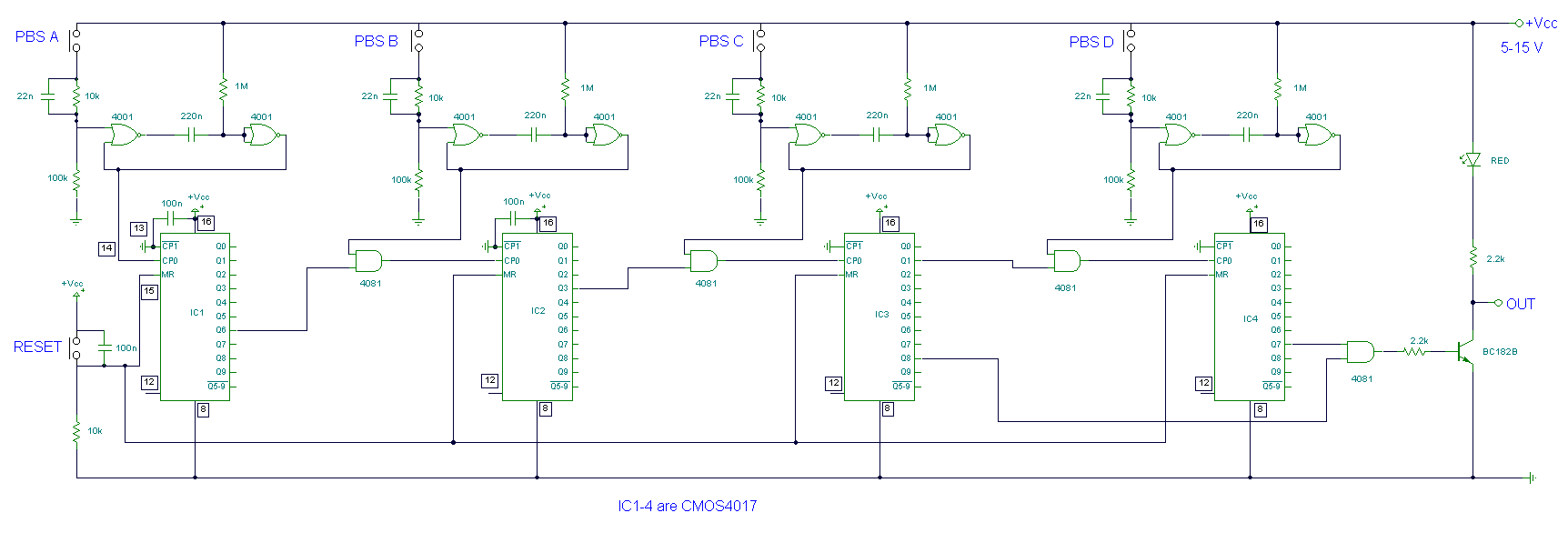
The circuit above makes use of the CMOS 4017 decade counter IC. Each depression of a switch steps the output through 0 - 9. By coupling the output via an AND gate to the next IC, a predefined code has to be input to create the output. Each PBS switch is debounced by two gates of a CMOS4001 quad 2-input NOR gate. This ensures a clean pulse to the input of each CMOS 4017 counter. Only when the correct number of presses at PBS A will allow PBS B to become active. This is similar for PBS C and PBS D. At IC4, PBS D must be pressed 7 times. Then PBS
C is again pressed 7 times, stepping from output 1 to output 8. The AND gate
formed around CMOS4081 then goes high, lighting the LED. The Reset switch can be
pressed at any time. Power on reset is provided by the 100n capacitor near the
reset switch. |
