|
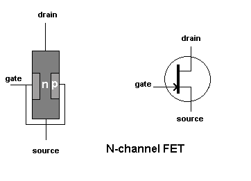 The field effect
transistor (FET) is made
of a bar of N type
material called the
SUBSTRATE with a P type
junction (the gate)
diffused into it.
With a positive voltage
on the drain, with
respect to the source,
electron current flows
from source to drain
through the CHANNEL.
If the gate is made
negative with respect to
the source, an
electrostatic field is
created, which squeezes
the channel and reduces
the current.
If the gate voltage is
high enough the channel
will be "pinched off"
and the current will be
zero.
The FET is voltage
controlled, unlike the
transistor which is
current controlled.
This device is sometimes
called the junction FET
or JUGFET or JFET.
If the FET is
accidentally
forward biased, gate
current will flow and
the FET will be
destroyed.
To avoid this, an
extremely thin
insulating layer of
silicon oxide is placed
between the gate and the
channel.
The device is then known
as an insulated gate FET,
or IGFET or metal oxide
semiconductor FET (MOSTFET) |