Basic Theory and Applications of MOSFET
|
Author: Prof. Dr. Marco
Gottardo |
 |
In this section we will study and see the practical use of these components in recent years have been increasingly successful thanks to the ease with which they can handle high power while being driven with minor signals also directly taken from the digital outputs of the microcontroller.
The excellent power / size ratio and power / price make it the ideal compound of the MOSFET for a high number of applications, especially for driving loads such as DC motors in continuous brush or large solenoids.
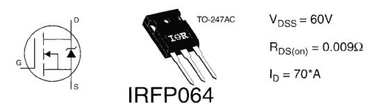
We see in the picture above the MOSFET IRFP064, produced by "INTERNATIONAL RECTIFIER". Its characteristic class "average" for these devices makes it useful for almost any application. As we can see this particular model has the housing (container) of type TO-247, and with which 'plug-in PCBs when we look in the libraries of CAD, but we can find or even MOSFETs in TO220 TO92. Obviously manage a specific power of each case.
From the electrical symbol we see that the terminals change their names to the elements than bigiunzionali, in fact these are:
- Gate: control terminal
- Drain: Terminal load
- Surce: reference terminal of the power mesh.
Just to make a comparison with a component of the NPN BJT, compared to the N-channel MOSFETs, it is at Gate-> Base, Drain-> Manifold, Surce-> Emitter.
The crossing of the channel DS by the electron current is encountering a single type of doping of the same channel, then the component is part of the so-called unipolar.
Since there are two types of polarity for the conductive channel (N or P) and that this channel can be already formed and the control takes place in throttling (pinch), or the channel is throttled and the control takes place in enrichment (enhacement), is can say that there are four configurations of the device and not two as' known for bipolar BJT components.
Unlike the bipolar components mosfet driver and voltage is not current, but this does not mean you will never enter into the current terminal driver.
A current pulse is established in the control terminal when the MOSFET is driven with a voltage pulse periodic or nonperiodic.
It is therefore having to analyze a transitional situation, sometimes repeated as a function of frequency command which essentially reflects the time constant which is being formed between the capacity existing between the substrate and the conductive channel (which acts as the dielectric when the voltage at armor and 'equal to zero and the test voltage and' that indicated in databook).
The ohmic value of the constant in question is' sought in the complex mesh gate that sometimes it becomes clear why only resistance, sometimes obtained by standard parallel synthesis. Iinstead, when the MOSFET is found driven with a signal unit step, if we neglect the transition phase and we can say that there 'current at the gate and the device is driven purely in tension.
In essence, the energy dissipation of the device takes part not only the current passing through the channel which meets the resistance of the same, in the case of saturation RDS on (the MOSFET shown equal to about 9 milli-ohm), according to the formula:
Pd = (RDSon * Ids ^ 2) * t
But also the heat loss due to the current charge / discharge capacity of the mesh control.
Quote from a forum robo87:
The gate is the control terminal of the MOSFET: varying the voltage between gate
and source changes the current flowing between the drain and source. In contrast
to the mosfet bjt is voltage driven, this leads to the fact that the gate
subjected to a fixed voltage does not absorb current. This characteristic of the
MOSFET is given by the fact that between the gate and the rest of the component
(part of silicon in which are formed the drain and the source), there is an
insulating layer of silicon oxide that electrically insulates the gate to source
and drain .
The name comes from this characteristic of MOSFET (Metal Oxide Semiconductor FET or FET and metal oxide semiconductor)
Practically between gate and source is formed a capacitor in which a terminal (armature) is connected to the metal gate, the second terminal / armor is instead connected to the part of silicon on which there are source and drain. The dielectric is the insulating layer instead of silicon oxide which separates the two armatures.
Based on these data it is clear how ever on the gate, with constant voltage, no current: as a real capacitor, the gate, initially uncharged, it is first crossed by electric current, then, when it is loaded, the current no longer circulates.
If the MOSFET is instead driven by a gate voltage pulse there will be a state of charge-> download-> charge-> etc.. of the capacitor gate / source, resulting in a non-zero gate current dependent on the frequency used and the gate-source capacity. The value of the current is related to that of the capacitive reactance or by the "resistance" introduced by the capacitor, whose value is calculated with the formula Xc = 1 / (2 * pi * f * C), where f is the frequency in Hz pulse signal and C the value of the capacity in Farad gate-source.
This fact is important when designing a circuit which uses MOSFET, because
the portion of the gate driver circuit must be sufficiently powerful to supply
the required current to the gate / capacitor to charge or discharge.
Unquote
Carefully reading the IRFP460 datasheet shows that the input capacitance Ciss
capacity
In test condition Vds 25V, f 1Mhz, Vgs is 0V of 2980 pf
That the Vgs max is + / - 30V with a maximum of 100nA Igss
So do a little 'calculations of mild
Let's say we drive the mosfet with our f 22kHz and 30V max Vgs replace the
formula: Xc = 1 / (2 * pi * f * C)
Xc = 1 / (2 * pi * 22kHz * 2980pf)
Capacity must be ** so pico farad 10 ^ -12 **
Xc = 2400 ohms approximately
Without this V / R = I => 30V/2400ohm = 0.0125 A
So in testing conditions, with maximum current drawn by the gate will be up to
12.5 mA, when drivers often should I make the distinction between low-frequency
(this is the case of the project in question) and high frequency, so you have to
do other calculations:
From the characteristic in the figure of the datasheet is located, in
correspondence of the VGS and VDS a
QG = x
At this point, also known the total time of transition (tt = td (on) + tr) is
calculated
gate current: Ig = Qg / tt = 1.13a
But they just do questri calculations when designing a class D switching
amplifiers