Terms of Eagle
|
Author: Prof. Dr. Marco
Gottardo |
 |
EAGLE ( http://www.cadsoftusa.com/freeware.htm ).
(This tutorial is a source and is available on the internet docenti.org)
These notes on the use of EAGLE, include:
- a concise tutorial reworked the tutorials on the site in English
- a tutorial on drawing a diagram
- a tutorial on the design of a printed circuit
- a complete sample schema and PCB.
Nobody wants to have the written claims of originality are inspired tutorial in English and French on the web and redesigned for use in a fourth class of a professional institute.
EAGLE is a powerful graphical editor for designing schematics and printed circuit boards.
It includes three modules: Schematic Editor, Layout Editor, Autorouter.
It can be used both in Windows 95/98/ME, Windows NT4/2000/XP is based on Linux kernel 2.x
We need a video graphics resolution of 1024 x 768 pixels minimum.
Eagle exists in several versions. The following are some basic details of the versions.
Professional Version
- Maximum work area (layout area) for PCB 64 x 64 inches (about 1600 x 1600 mm)
- printed circuit boards up to 255 layers (layers)
- full support for SMD components
- rotation at any angle
- up to 99 sheets (sheets) for each diagram
- autorouter integrated, without restriction of any placement
- autorouting up to 16 signal layers (with customizable direction)
Standard Version
- maximum working area 160 x 100 mm (about 6.3 x 3.9 inches).
- maximum of four layers: upper (top) lower (bottom) 2 internal (inner layers).
Version Light Edition (Freeware)
Available as Freeware (for testing and evaluation):
- maximum working area 100 x 80 mm (about 3.9 x 3.2 inches).
- only two layers, top and bottom
- the circuit diagram is composed of a single sheet.
Products are still files for production (Gerber and drilling)
They may be viewed and printed larger projects.
When you install the freeware version does not need a User License Certificate.
You choose the option: Run as freeware.
After the standard installation, EAGLE allows you to customize performance, such as the configuration menus, function keys or the colors on the screen.
You use the Options menu or the various editor windows.
EAGLE User Interface.
Internally EAGLE is designed to run commands as a string type.
The user will normally use the mouse on the menu and toolbars (toolbar).
It is not necessary to know the language of internal control, however, this mode allows you to type a command in a text or to read the commands in a file. You can assign command strings to function keys (ASSIGN command) and run the script (SCRIPT command).
Some commands are given in combination with the Shift, Ctrl, Alt
Alt + F2 means that the Alt key is held down while you press F2, then release both buttons.
Of course the same command EAGLE can be given with the keyboard, clicking on the icons of commands, click on menu items.
For example, to execute the MOVE command, you can:
Click on the icon
MOVE type on the command line followed by Enter
press the F1 function key assigned to the command MOVE
select the menu item: Edit / Move
Normally EAGLE does not distinguish between lowercase and uppercase.
When the mouse cursor is positioned for a time on an icon, is a descriptive help text (Bubble Help text).
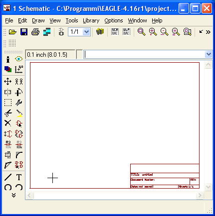
Window Work:
From top to bottom:
- Title with information about the version of EAGLE
- Menu bar (menu bar)
- Action Bar (action toolbars)
- Barra dynamic (parameters and coordinates) + command line (command line)
- On the left command bar (toolbar command)
(You see the Bubble Help text for the command WIRE)
- status bar (status bar): indicates the current command
The bars can be hidden / shown using the menu Options / User interface ..
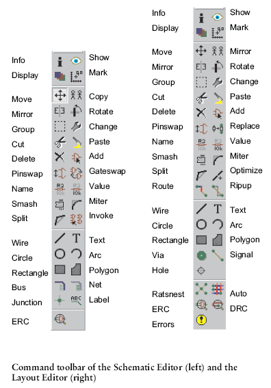
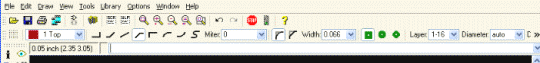
Bar commands Schematic Editor (left) and the Layout Editor (right)
Control Panel
Opening of EAGLE, is the Control Panel. Allows you to load and save projects. Right-click on Projects With a menu that allows you to create a new project.
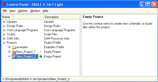
Each entry opens with a double click. For example, clicking on Libraries is its content, selecting an object it appears the description.
The Control Panel allows the normal Drag & Drop: If you right click on an item, the context menu appears with the normal operations of print, open, copy, etc..
EAGLE Files
The types of files that appear in EAGLE are:
Board Layout Editor *. Brd
Schematic Schematic Editor *. Sch
Library Library Editor *. Lbr
Script File Text Editor *. Scr
User Language Program Text Editor *. Ulp
Any text file Text Editor *.
Backup Files
EAGLE creates backup files, up to a maximum of 9, files of the schematic, board, library files. They are saved with extensions changed:
. Brd becomes. B # 1,. Becomes sch. S # 1. Lbr becomes. The # 1.
All original settings are back to the menu Options / Backup.
Creating a Project Eagle.
File - New Projects
A new folder under the heading Projects, which will contain all project files, you can delete and rename using the context menu.
With right click on the folder you open the context menu, with which to create new patterns of all types (sch, brd, etc..)
In the Examples folder - Tutorial there are some demo files. sch and. brd. that can be used to practice.
To avoid altering the original copy in the new project folder
Each file can be opened by double-clicking.
Drawing of a wiring diagram
Select the project folder.
Open the project (File menu or contextual menu). Create a new schematic file.
You see a blank sheet.
The standard grid is 0.1 inches (100 mils, 2.54 mm.). Do not change it! Symbols and links must be placed on this grid.
Adding a Frame to the sheet
The blank sheet must have a border (frame).
In the command line write: add.
In the list that appears choose the voice frames, select one of the predefined formats.
(For a horizontal A4 sheet can be used:
A4L_LOC, DINA4_l, LETTER_L)
Giving OK, the frame appears "attached" to the cursor: place in space, with the angle in the lower left point pù bottom of the paper, left click to place it, click on Stop to exit the add; type ALT + F2 (or fit between the zoom commands) to see the entire frame. Save the empty scheme.
The frame contains empty fields (title, review, document number) to fill out some.
Both TITLE and DATE fields are filled automatically by the program when you save the file.
To enter new text in the command bar on the left click the icon TEXT, type text and place. To change the size of the icon select CHANGE, then SIZE (STOP mode by selecting the text).
Given that EAGLE runs on the command line, you can also type: CHANGE SIZE 0.17, and hit Enter on the corner to the lower left of the text.
Warning: Use the decimal point.
Draw and edit the circuit
ADD: command to add the components, without changing the grid of 100 mils.
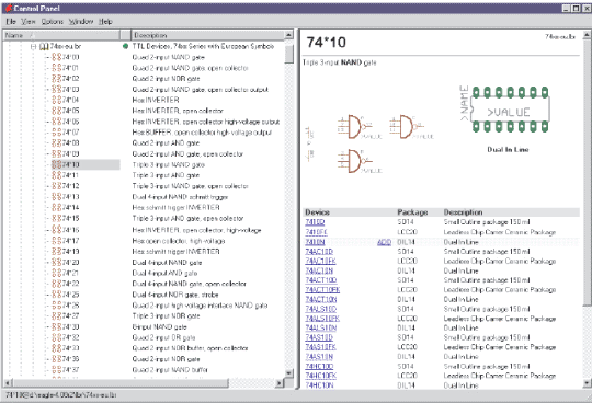
Libraries should be explored carefully.
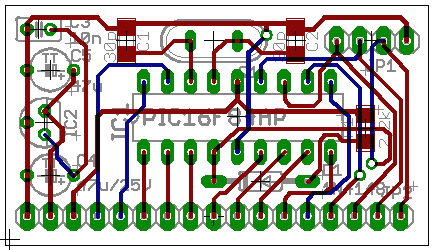
For example, some components present in the diagram demo1.sch are:
| Part | Value | Device | Package | Library | Sheet |
| C1 | 30p | C-EUC1206 | C1206 | rcl | 1 |
| D1 | 1N4148 | 1N4148 | DO35-10 | diode | 1 |
| IC1 | PIC16F84AP | PIC16F84AP | DIL18 | microchip | 1 |
| JP1 | PROG | PINHD-1X4 | 1x04 | pinhead | 1 |
The initial difficulty is to identify the exact component you want (through hole or SMD, horizontal or vertical, with the desired pitch between pins etc..) Through the many libraries available that use industrial designations.
MOVE: To move and position the components (MOVE switch to move and click on the component, right-click to rotate, move, press Enter). Be careful when moving a component over another if incorrect connections are created automatically. When you stand close to or overlapping of two components, the cursor turns into a 4-arrows, and you have to make a choice: you choose with the left click on the highlighted component, right-click with the next one.
COPY to duplicate components, without reloading the library.
CHANGE NAME and VALUE: to change the name and values of the components:
DISPLAY: Allows you to disable the schema components and usually has disabled the layer 93 (Pins).
NET: after placing the components, for making connections. (Do not use the WIRE command, serving instead to establish the margins of the printed circuit!). By right-clicking, it toggles the orthogonally or diagonally to draw the connection. If it terminates the connection exactly on a point of connection, as the leg of a component, the net is terminated, otherwise moving the mouse continues.
Two points connected to a net having the same name are electrically connected, even if it is not designed a continuous connection. To ensure that the components are connected with the DISPLAY command - PIN can be seen as green circles exactly where to connect.
LABEL: to bring up the diagram as a link (net or bus), you can change the font used with CHANGE.
DELETE: position and click on the component, if you want to delete a link, it will be deleted one segment at a time, to erase an entire link, also press the Shift key (Shift)
UNDO, REDO: undo / redo the last action
GROUP: the command applies to a group of objects
JUNCTION: Adds a junction (node) in a link. Normally not needed because the default is enabled Automatic Sept. junction (see Options / Set / Misc), so if you draw a link on an existing node is created automatically. The command is used to add more nodes.
SHOW: shows details of the objects. It 's quite nice because when used on a component of the package and it also provides the library, if used on a route shows all connections that have the same name, you can type on the command line as a shortcut to search and it is highlighted. To end the command, click on STOP and then redraw the diagram with the F2 key (View / Redraw).
SMASH: when rotating a component, it also rotate together with the code (reference designator) and the value. The SMASH command allows you to turn and reposition symbol and value, regardless of the position of the component.
You can also use Change / Size to vary at will the appearance of the writings.
To complete the scheme should be added to the supplies, +5 V, V +, GND, from the library supply1.lbr.
The symbols are the power supply signals; are controlled in a particular way by the command ERC (Electrical Rule Check) in the process of checking the accuracy of the pattern.
ERC: The command is used to check for errors in diagrams. Messages are generated that contain real errors (errors) and warnings (warnings): Messages are contained in a file that has the same schema name and extension. Erc. and are displayed automatically.
An example of warning:
WARNING: Sheet 1/1: POWER Pin IC1 VSS connected to GND
WARNING: Sheet 1/1: POWER Pin IC1 VDD connected to +5 V
warns that called VSS and VDD pins are connected to GND and +5 V. The message can be ignored if this was done intentionally.
Warning: ERC points to the possible errors! It must also be able to interpret them correctly.
BUS: to draw a multilink using a particular symbol: a link from which more often there are several links to individual components.
As an example, load the design bus.sch from the / eagle / examples / tutorials, where there is a bus that brings together 13 signals. The bus name determines the signals it contains: the name EN, VALVE [0 .. 11] agreed with the NAME command means that it contains the signal EN and the signals from VALVE0 to VALVE11.
The bus is just a graphic: the connections are established with the NET command.
In the scheme bus.sch are still to be made of links, such as the signal VALVE0 must be connected to pin 16 of IC7. To connect: type the command NET, positioned on the bus at the point from which to start the connection, left click, a drop down menu appears with the names of all signals, VALVE0 choose, choose the curvature of the connection (wire bend) to right angles or obliquely to bring the connection to pin 16 of IC7, exit the Stop command.
To bring up the name of the connection use the LABEL command.
Automatic Forward & Back Annotation
This process ensures that the schema and the PCB are compatible (consistent), ie a list of links, components, values are identical.
The process is activated by EAGLE automatically when you load a diagram and a circuit board having the same name and are in the same directory. The result is shown in a text window, so as to manually correct the differences.
To ensure a perfect correlation between diagram and printed circuit board, keep open both files. And sch. Brd. In this way, any variation in the key results in an immediate change in the printed circuit board. Some changes may be made either in the diagram in circ. print (eg name of the components), others, such as the addition of components, only the diagram.
Generation of a printed circuit board (board) from a schema (schematic).
Load the schema to be transformed into the board.
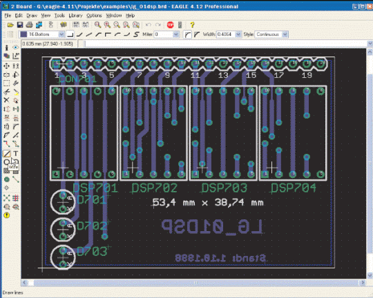
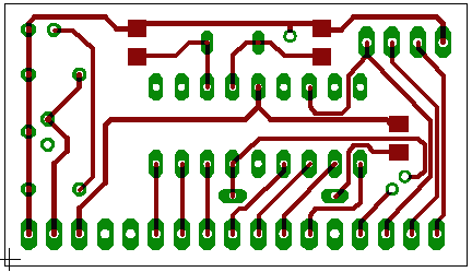
Click on the icon of the Control Board in the action toolbar: it generates a file that has the same schema name and extension. Brd. Layout Editor window appears with an empty board defined by a profile consisting of wires. Outside the board on the left are all connected to each other with flying leads "elastic" (airwires) to be placed inside the empty area. The dimensions are 3.90 x 3.20 inches around, the maximum allowed by the free version. With the MOVE command, however you can reduce the size of the PCB.
Placement of components:
MOVE to move the components, they took with them the flying colleamenti (airwires).
Upon completion of the placement, with the command RATNEST you can see the path of minimum flying connections for optimal positioning.
Use of 'Autorouter (Automatic tracking of slopes)
Can be started by the autorouter at anytime. However it is not good to entrust automatic routing solution of all problems are typically drawn by hand the slopes for the supplies (considering the greater thickness required for the mass) and connections are considered critical.
If you want to see how the autorouter solve the circuit, click on AUTO. It seems the setup dell'autorouter: by default the grid is set at 50 mils (but can be changed), the preferred direction of red runs (top layer component side) is vertical, while for blue runs.
(Bottom layer solder side) is horizontal.
Auto-routing schemes for small and virtually immediate.
If the result does not satisfy, you can erase the tracks RIPUP with the command: it is possible to delete some or all, then you must click on GO (semaforino little action on the toolbar next to STOP). To ensure correct deleted tracks desired, give the command to see RATNEST airwires. After the cancellation raises the autorouter.
The traces made manually are not shifted dall'autorouter.
After dell'autorouting, a message appears with the percentage of runs made. With the command RATNESTS you view the tracks that are not tracked.
Manual routing
No autorouter will place ever tracks just as you want, so you must resort to manual routing.
Give the ROUTE command to turn a airwire in a track. Click on the beginning dell'airwire, left click at the end of each segment, double-click left to finish the track. At the end of a runway the ROUTE command is still active, so you can track another track from the beginning.
When tracing is enabled bar parameters (parameter toolbar) where the layer is
(In figure 1 Top red slope), the angles possible for slopes, the radius of curvature, the thickness (in the figure Width: 0.066 inches), the type of hole (in the shape of a square shape). During tracing you can change all the parameters, if you decide to change layer, EAGLE automatically inserts a hole.
The MITER command is used to connect sections of curved and straight tracks.
The procedure that leads to the complete definition of the printed circuit comprises several steps:
- moving segments of track and components with MOVE and SPLIT
- RIPUP use the command to change the location of the slopes
- use DELETE to erase signals (only without the Forward & Back annotation),
- change the package of components with CHANGE or REPLACE PACKAGE
- SMASH used to place the texts of the components that have undergone a MOVE
- fillet curved tracks.
Some details of the various commands:
MOVE
If you select the end of a track that moves, if you select a track in the middle of all the moves in parallel. If you press the Ctrl straight track becomes an arc.
While in the MOVE command, you can turn 90 degrees right-clicking the object, or angle desired by the value that appears in the parameter toolbar.
GROUP
Allows you to select different objects to change the attributes or move them all together.
Type then click GROUP repeated claims, or moving the mouse, draw a polygon around objects, ending with right click: Objects are highlighted. The MOVE command operates on all or CHANGE. Going out with right click.
SPLIT
Adds a curve in a track.
CHANGE
you can type the desired changes (width, layer) but is much more convenient to use the parameter toolbar.
RIPUP
If you want to turn a track on a signal in a airwire, type the name of the signal in the command toolbar.
In particular we want to remove all tracks except power, we can turn RIPUP and type.
! GND VCC
SHOW
serves to highlight airwires tracks or components, because they are immediately visible on the screen
REDRAW or F2
rinfesca screen.
DISPLAY
The screens contain EAGLE objects located in different layers (layers). The set of layers determines how to print or use the project results. Giving the DISPLAY command displays a list of layers. For example the layers Top, Hall and Via are used to generate a film for the engraving of the component side of the printed circuit, while the layers Bottom, Hall and Via are used for the solder side.
Pad layer contains the holes (through-holes) for the components not SMD, the layer contains Via the through holes to allow a track to pass from one face to another.
The other film needed is that related to screen printing, containing only the view of the components. In general, for simple circuits screen printing is done only on the component side.
Selecting / deselecting the different layers, you may want to get printed.
- To get the screen printing side components: 1 deselect the layers Top, Bottom 16, 17 Pads, Vias 18. There remain only the profiles of the components and all the writing (names and values). If you do not want anything to appear in the screen printing, you can uncheck the other layers as desired.
- To obtain the release of only the component side tracks: Clear Bottom 16, 21 tPlace (silk screen upper side), 39 tKeepout (profile SMD)
- To obtain the release of only the solder side tracks: 1 clear top, 22 bPlace (silk screen bottom side).
Given that the background (background) of the PCB is black by default, in the Options menu - User interface can be
choose to color the white background layout.
only tracks the component side
across the board
Ground planes
on the printed circuit areas may appear entirely filled with copper, areas or zones of mass for heat dissipation.
You plot with RECT or POLYGON commands with parameters to be chosen for the parameter toolbar.