|
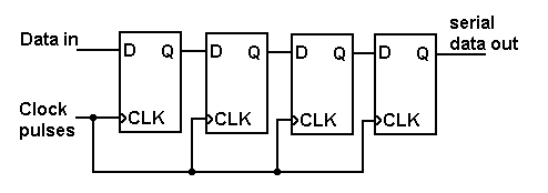 The diagram shows four flip-flops connected to form a SERIAL IN, SERIAL OUT shift register.
Upon the
arrival
of a
clock
pulse,
data at
the D
input of
each
flip-flop
is
transferred
to its Q
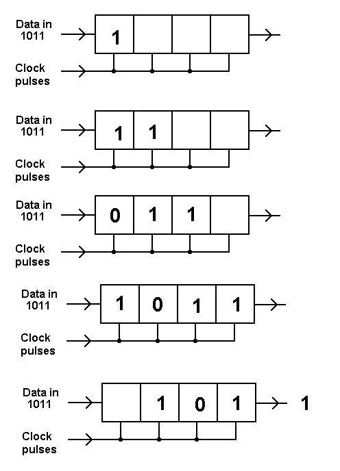
output. At the start, the contents of the register can be set to zero by means of the CLEAR line. If a 1 is applied to the input of the first flip-flop, then upon the arrival of the first clock pulse, this 1 is transferred to the output of flip-flop 1 (input of flip-flop 2). After four clock pulses this 1 will be at the output of flip-flop 4. In this manner, a four bit number can be stored in the register.
After
four
more
clock
pulses,
this
data
will be
shifted
out of
the
register.
 |