|
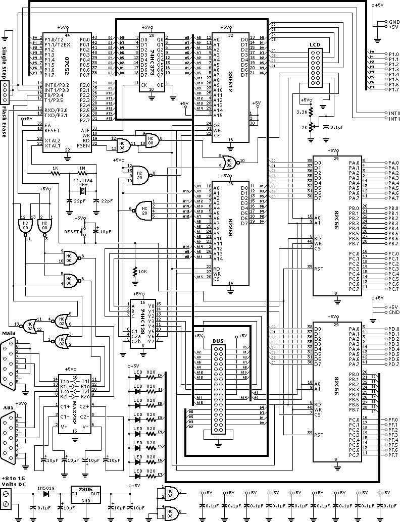
Click on diagram for better view This schematic is provided in the hope that it will be useful, but without any warranty, not even a warranty of merchantability or fitness for a particular purpose. The address bus in this schematic is connected in an unusual way, which is optimized for simpler point-to-point wiring and board layout. For anyone building the board using wire-wrap or hand soldered point to point construction, this wiring scheme makes for much less clutter in the wiring if the chips are positioned similarly to the layout on the printed circuit board.
This unusual address bus wiring works. The 74HC373 chip (U2) is 8 identical flip-flops, so it does not matter which one is used for each line. On the RAM (U3) and Flash ROM (U4) chips, all data that is stored in these chips is written by the 87C52 chip (U1), so it does not matter which physical location within the chip is mapped into each location within the CPU's address space, because each read from these chips will return the same data that was written from a previous write. Some readers have felt that it's "just not natural" to connect any other way than P0.0-D0-Q0-A0, P0.1-D1-Q1-A1, and so on, but it does indeed work. For a historic example, Woz used a very creative address bus connection scheme in the Apple ][ to automatically do DRAM refresh with his video refresh reads. Because he arranged the address pins a certain unusual way, every video mode accessed each DRAM row several times per video refresh, so he didn't need to add the cost and space of the usual DRAM refresh circuits (he interleaved video and cpu memory access, since the 6502 spends half its time not fetching anything). It works, and Apple sold millions of them! The MAX232 chip (U9) is shown with C3, C4, C5, and C6 as 1 µF, but the board is usually built with 10 µF capacitors (as shown in the parts list below). Either will work. C6 is connected to ground. In the sample circuit within the datasheet, it is connected to Vcc. Either connection will work. This connection causes charge-pump current flow through C8 and C10, but it avoids coupling the Vcc line to the V+ pin (high frequency digital switching noise, relative to ground, despite C11-C17). The V+ pin is ultimately connected via the MAX232 driver to the RS-232 cable.
Parts
List
| Quantity | Reference | Description |
|---|
| 1 | | IC, 87C52, Microcontroller (program with PM21_2F4.HEX), PLCC-44 | | 1 | | IC, 62256, SRAM, 32Kx8, DIP-28 | | 1 | | IC, SST39SF512, Flash ROM, (39F010, 39F020 ok) PLCC-32 | | 2 | | IC, 82C55, Programmable Peripheral Interface, PLCC-44 | | 1 | | IC, MAX232, RS-232 Interface, +5 Volt, DIP-16 | | 1 | | IC, 74HC00, Quad NAND Gate, DIP-14 | | 1 | | IC, 74HC02, Quad NOR Gate, DIP-14 | | 1 | | IC, 74AC08, Quad AND Gate, DIP-14 (use AC family for 22 MHz) | | 1 | | IC, 74AC20, Dual 4-input NAND Gate, DIP-14 (use AC family for 22 MHz) | | 1 | | IC, 74HC138, Decoder, 3 to 8, Active Low, DIP-16 | | 1 | | IC, 74HC373, Octal D Flip-Flop, DIP-20 | | 1 | | IC, LM7805, Voltage Regulator, +5 Volts, TO-220 | | 1 | | Crystal, 22.1184 MHz, HC49/SU, Parallel 20pF | | 8 | | LED, T-1 3/4, Red, Low Current Ultra Bright | | 2 | | Capacitor, 22pF | | 11 | | Capacitor, 0.1µF | | 8 | | Capacitor, 10µF, 35V | | 1 | | Diode, Schottkey, 1N5819 | | 8 | | Resistor, 820, 5%, 1/4W | | 1 | | Resistor, 1k, 5%, 1/4W | | 1 | | Resistor, 3.3k, 5%, 1/4W | | 1 | | Resistor, 10k, 5%, 1/4W | | 1 | | Resistor, 1M, 5%, 1/4W | | 1 | | Trim POT, 2k, 1 Turn | | 1 | | Pushbutton, Momentary Contact, 6 mm, 4 or 5 Pin | | 1 | | Connector, Terminal Block, 2 Conductor, 5.08 mm | | 2 | | Connector, D-Sub 9 Pin Socket (Female), PCB Right Angle | | 1 | | Socket, 2x7, 0.1 Inch Spacing | | 1 | | Header, 4 pin, 0.1 Inch Spacing | | 4 | | Socket, DIP, 14 pin, 0.3 inch | | 2 | | Socket, DIP, 16 pin, 0.3 inch | | 1 | | Socket, DIP, 20 pin, 0.3 inch | | 1 | | Socket, DIP, 28 pin, 0.6 inch | | 1 | | Socket, PLCC, 32 pin | | 3 | | Socket, PLCC, 40 pin | | 1 | | Heatsink, TO-220, 0.7x0.7x0.35 | | 1 | | Screw, 4-40, 3/8 inch | | 1 | | Nut, 4-40 | | 1 | | PC Board, DEV_PCB_BARE |
How The Address Decoding Logic Circuitry Works
The basic idea is that some logic chips connect to the upper address bits and they assert on of the chip select signals, depending on what memory range the processor is accessing.
The A15 signal goes directly to the RAM, so the RAM gets selected for all addresses where A15 is low (0000 to 7FFF). A11 to A14 go to a 4-input NAND gate. That gate outputs low when all four signals are high, and its output is low in all other cases. That gate and the A15 signal go to the other 4-input NAND gate and to the 74HC138 chip. When A15 is high, and any of A11 to A14 are low, the other 4-input NAND gate drives the flash rom chip select low. That means the flash rom is enabled from the range 8000 to F7FF. Those same two signals also go to the 74HC138 chip's G1 and G2a inputs. The 74HC138 only drives one of its outputs low when G1 is high and when G2a is low. That means the 74HC138 chip drives one of its 8 signals in the range of F800 to FFFF. The three address inputs to the 74HC138 are connected to A8, A9 and A10, so that each of those signals corresponds to a 256 byte range. If you follow where each one goes, you'll see they correspond to the memory map for the periperals.
Most of the chips are designed to connect directly to the bus, so all that's needed is to connect their address pins to the lower pins of the address bus, their data pins to the data bus, and their write and output enable pins to the WR and RD/PSEN signals. All the chips see all those signals, but only the chip that gets a low signal on its chip select pin will communicate with the processor. All the other chips remain silent. The 8051 provides the address information before it asserts RD, WR or PSEN to cause the chip to communicate, and the logic gates are chosen so that the chip select signals are generated before the 8051 strobes on of those control signals.
The LCD is the one device that is a bit different. Most bus interface devices require the address signals first, then the chip select, and then the RD or WR control signal. The LCD instead requires its address (register/data select), read/write select, and data signals first. Then an active-high enable signal is given to the LCD to make it execute the bus cycle. To accomplish this, the R/W signal of the LCD is connected to an address pin, as is the RS (register/data select). This way those signals are asserted first and maintained throughout the bus cycle. This means that separate memory locations must be used to read from and write to the LCD. The three control signal are AND'd together and fed to a NOR gate with the active-low chip select, so that the LCD will get an active high enable signal that begins well after the address pins are stable (as is required by most common LCDs).
About The Memory Size (How To Add More Memory)
Frequently I receive email about making modifications to this design to provide more memory. There are some important considerations to using more memory, but it certainly is possible... the mp3 player project uses 32 megabytes! But using more memory requires careful consideration.
The most important factor is that the 8051 processor has a 16 bit address space. This means the processor can never "see" more than 64k of memory. Actually, the 8051 has three memory spaces, 256 bytes of internal RAM, and two 64k byte external spaces, one for data and the other for executable code. The executable code space is read-only (PSEN signal), so there is really only one writable 64k address space. This design uses an AND gate (74AC08) to combines the two spaces together, which makes the board simpler to use and of course is needed to allow writing to the memory during code download. So in the end, there is really only a 64k address space to use.
A common approach to using more memory is to connect the memory as shown above, and then to connect the higher address bits (A16, A17, etc) to port pins. This is called "bank swapping", because it effectively provides multiple banks of memory and only one is "visible" to the processor at any one time. The banks are "swapped" by changing the port pins that connect to the upper address bits.
In the schematic above, the 39F512 flash rom is actually 64k of memory, but only 30k is available to the user (the chip select logic does not assert CE, pin 22, so that the LCD, 82C55 and chip select signals can use the upper 2k of the memory map). A simple approach to using 60k of flash memory would be to disconnect A15 (pin 3) from +5V and attach it to one of the port pins. Likewise, a 39F040 chip could be substituted for the 39F512, and then A16, A17, and A18 could be attached to additional port pins to provide sixteen banks of 30k or a total of 480k of flash memory.
A
similar
approach
could be
used
with the
RAM
chip, as
there
are 128k
and 512k
RAM
chips.
These
larger
RAM
chips
have 32
pins
instead
of 28
pins,
but
their 28
common
pins
have
similar
functions,
so only
a few
extra
pins
need to
be
connected.
Again,
connecting
upper
address
bits to
the port
pins
would
allow
the
memory
to be
"bank
swapped.
|