|
Click
on
diagram
for
better
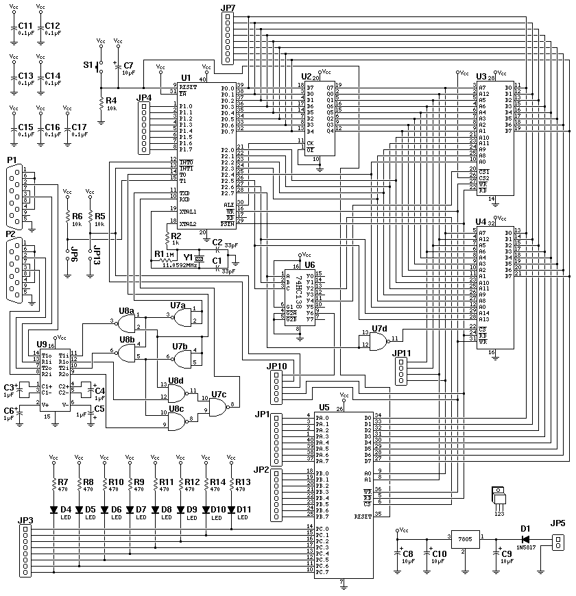
view The address bus in this schematic is connected in an unusual way, which is optimized for simpler point-to-point wiring. For anyone building the board using wire-wrap or hand soldered point to point construction, this wiring scheme makes for much less clutter in the wiring if the chips are positioned
similarly to the layout on the printed circuit board. Very few wires cross over one another. This also makes the PC board layout a bit simpler, allowing wider traces and fewer vias.
This unusual address bus wiring works. The 74HC373 chip (U2) is 8 identical flip-flops, so it does not matter which one is used for each line. On the RAM (U3) and Flash ROM (U4) chips, all data that is stored in these chips is written by the 87C52 chip (U1), so it does not matter which physical location within the chip is mapped into each location within the CPU's address space, because each read from these chips will return the same data that was written from a previous write.
Some readers have felt that it's "just not natural" to connect any other way than P0.0-D0-Q0-A0, P0.1-D1-Q1-A1, and so on, but it does indeed work. For a historic example, Woz used a very creative address bus connection scheme in the Apple ][ to automatically do DRAM refresh with his video refresh reads. Because he arranged the address pins a certain unusual way, every video mode accessed each DRAM row several times per video refresh, so he didn't need to add the cost and space of the usual DRAM refresh circuits (he interleaved video and cpu memory access, since the 6502 spends half its time not fetching anything). It works, and Apple sold millions of them! The MAX232 chip (U9) is shown with C3, C4, C5, and C6 as 1 µF, but the board is usually built with 10 µF capacitors (as shown in the parts list below). Either will work. C6 is connected to ground. In the sample circuit within the datasheet, it is connected to Vcc. Either connection will work. This connection causes charge-pump current flow through C8 and C10, but it avoids coupling the Vcc line to the V+ pin (high frequency digital switching noise, relative to ground, despite C11-C17). The V+ pin is ultimately connected via the MAX232 driver to the RS-232 cable.
Memory Map
0000 - 1FFF PAULMON2 Monitor
2000 - 3FFF SRAM
4000 - 5FFF 82C55 I/O Chip
4000: Port A (read or write)
4001: Port B (read or write)
4002: Port C (read or write)
4003: Configure (write only)
6000 - 7FFF User Expansion (Y6 signal assert low)
8000 - FFFF Flash ROM
All memory on the rev 3 board is read using MOVC (code space). The RD signal is not connected, so MOVX may not be used to read the memory.
Connector Pinouts
 | |
Pinout Diagrams, Contributed by Kaushik B. M. (kaushikbm@hotmail.com) |
Parts List
| Quantity | Reference | Part |
|---|
| 2 | C1,C2 | Capacitor, 22 to 33 pF | | 8 | C3,C4,C5,C6,C7,C8,C9,C10 | Capacitor, 10 µF, 35V | | 7 | C11,C12,C13,C14,C15,C16,C17 | Capacitor, 0.1 µF | | 1 | D1 | 1N5819 | | 8 | D4,D5,D6,D7,D8,D9,D10,D11 | LED, T-1 Size | | 1 | R1 | 1MEG | | 1 | R2 | 1K | | 3 | R4,R5,R6 | 10K | | 8 | R7,R8,R9,R10,R11,R12,R13,R14 | 470 to 1k (depending on LED brightness) | | 1 | U1 | 87C52 (or equiv), pgm w/ PAULMON2 v2.1 | | 1 | U2 | 74HC373 (Octal Latch) | | 1 | U3 | 6264 (or similar 8K x 8 SRAM) | | 1 | U4 | SST39F512 (Flash ROM) | | 1 | U5 | 82C55 (I/O Chip) | | 1 | U6 | 74HC138 (3:8 Decoder) | | 2 | U7,U8 | 74HC00, Quad NAND Gate | | 1 | U9 | MAX232 | | 1 | Y1 | 11.0592 MHz Crystal | | 2 | P1, P2 | DB-9 Female Connector, Digi-Key Part # A2100 | | 1 | JP5 | Molex 2 Pin Header w/ Locking Ramp | | 2 | JP6,JP13 | 2 Pin Header (a single 4 pin may be used) | | 1 | - | 7805, 5 Volt Linear Regulator | | 1 | - | Heatsink | | 1 | - | Machine screw, 4-40, 1/2 inch | | 1 | - | Nut, 4-40 | | 2 | - | 14 Pin DIP Socket | | 2 | - | 16 Pin DIP Socket | | 1 | - | 20 Pin DIP Socket | | 1 | - | 28 Pin DIP Socket | | 1 | - | 32 Pin DIP Socket | | 2 | - | 40 Pin DIP Socket |
|