|
Author : Myke Predko
Alphanumeric LCD displays have become very popular for microcontroller applications because they can add a lot to a project in a variety of different ways. A text message giving the user instructions as well as feedback can make the application seem much more "professional" and easy to use. I like to use LCD's to help debug applications, with breakpoints set to display variable and I/O conditions and they are a lot cheaper than using a microcontroller emulator. To top it off, surplus LCD's can be found for a dollar or less.
The most popular LCD interface is the Hitachi 44780 based LCD controller chip which provides a fairly easy to work with interface and low power consumption. The major drawback of the interface is the perceived complexity of working with the interface. This perception has been promoted by the lack of good (i.e. well translated) and accurate datasheets and web site information.
Often the biggest stumbling block to using alphanumeric LCD displays is the number of pins required to control them. For the Hitachi 44780, twelve pins are required from the microcontroller to interface to the display for it to work in eight bit mode. For many smaller microcontrollers, twelve pins are not available or will be better served in the application. To be fair, this can be reduced to six by using the 44780's "Four Bit" mode, but this can still be more than acceptable for most applications.
A popular solution that only requires one pin from the microcontroller to the LCD is the use of "Serial LCD Interfaces" to the data and signals necessary for the Hitachi 44780 controllers.
Many of these products (such as the SLI-OEM) are excellent and can provide useful product interface and debugging information. The only drawback to them is the need for properly timed NRZ serial data which may be difficult or even impossible to guarantee in some applications.
In this case, different approaches have to be made. The most popular one is to use synchronous serial data (requiring a "clock" and "data") pin to load a serial-in/parallel-out shift register with the data bits and "R/S" pin information. The "E" Strobe Pin is driven directly by the microcontroller to latch in the data from the LCD. This is shown in the diagram below:

The project presented in this article is an enhancement of this circuit. By combining the shift register's "Data Line" with the most significant bit of the shift register, the "E" Strobe can be implemented without resorting to a separate line for the function. The 1 K resistor and diode act as an "AND" gate. A schematic of the circuit is shown below.
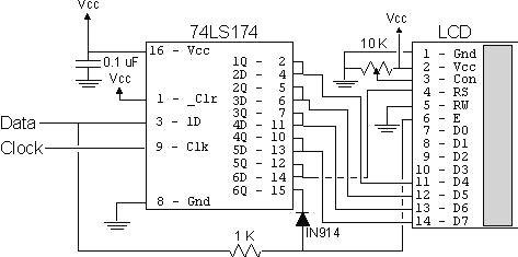
The operation of the resistor/diode "AND" gate may not be immediately obvious. When the shift register bit is low, the diode pulls the connection to the "E" pin low. When the shift register bit is high, the diode will not cause any current flow from the connection at the "E" pin to the shift register. The resistor from "Data" to the "E" pin is a current limiting resistor. When the shift register bit is low and the data bit is high, then the current through the resistor will be limited to 5 mA (for a 5 Volt logic application). At the "Data" side of the resistor, the voltage will still be high, even though the diode is pulling the "E" pin low.
When both the "Data" line and the shift register bit are high, the "E" pin will be high. The "AND" circuit could be a TTL two input AND gate (such as a 7408), if you have an extra one available for your application. When I originally created this circuit, I used the same two transistor and two resistor circuit that I used for the 89C2051 emulator in "Programming and Customizing the 8051 Microcontroller". I saw this "AND" equivalent circuit in an old copy of "Electronics Now" and found that it worked well in this application.
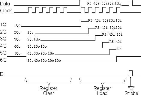
To load the shift register, it first has to be cleared to ensure that the "E" will not be strobed to the LCD inadvertently. This is done by first shifting in six "0"s to make sure that while the correct data is being loaded into the shift register, no "high" voltage level is passed to the "E" pin of the LCD.
Once this is done, the data can be shifted in. The diagram below shows how the shift register is initially cleared and then loaded with the data to be strobed
(using
"E")
into the
LCD:
The application code, "2wirelcd.asm" is an assembler source file written for the PIC16C84. The file is written to be used with the "MPASM" assembler built into Microchip's "MPLAB". I wrote the code with the idea that it should be easily portable to any low-end or mid-range PICMicro without modification.
For the two I/O pins ("Data" and "Clock"), I "defined" them to allow you to use virtually any pins in your PICMicro application. I say "virtually any" because PORTA pin 4 (also known as "RA4") is of "open drain" configuration and cannot source a positive voltage. The code itself is a very straightforward example of writing a 4-bit LCD application which displays the string "Hello" on the LCD display. The important difference between this code and a straight 4-bit LCD output is the "NybbleOut" subroutine, which is called twice by each of the "SendCHAR" and "SendINS" subroutines (which send characters and instructions, respectively, to the LCD).
"NybbleOut" first drops the "Data" line and then strobes the "Clock" bit six times to clear the shift register. Next, a "1" is strobed in, followed by the "R/S" pin value, which is stored in the PICMicro's "Carry" flag. I used Carry for this purpose because in this application I used RA0 and RA1 as the output pins and to simplify the operation of the code, I shift PORTA with Carry loaded with the "Data" Pin Value.
If this is not possible in your application, then "NybbleOut" should be changed to the following code. I have marked changed lines with "####' in comments.
NybbleOut2 ; Send a Nybble to the LCD
movwf NOTemp ; Save the Nybble to Shift Out
swapf NOTemp ; Setup to Output to the High Part of the Byte
movlw 6 ; Clear the Shift Register
movwf Dlay
NO2Loop1
ClockStrobe
decfsz Dlay
goto NO2Loop1
movlw 5 ; #### - Now, Shift out the Data with the "RS" Bit
movwf Dlay
bsf Data ; Put out the Gate Bit
ClockStrobe
NO2Loop2
bcf Data ; #### - Clear the Data Bit (which is the Clock)
btfsc STATUS, C ; #### - If the Bit to be output is a "1", Shift it Out
bsf Data
ClockStrobe
rlf NOTemp ; #### - Shift the Next Bit into the Carry Flag
decfsz Dlay
goto NO2Loop2
EStrobe ; Strobe out the LCD Data
return
The
only
point to
notice
with
this
code is
that the
"E"
strobe
will
become
active
on the
last bit
if the
least
significant
data bit
is high.
This
lack of
"settling
time"
before
"E" is
active
does
violate
the
"true"
44780
specification,
but I
haven't
found it
to be a
problem
when
I've
built
this
circuit.
|