Let's go PIC - Digital I/O
|
Author: Prof. Dr. Marco
Gottardo |
 |
Part Three: New C16 programming course for PIC development system based on PIC Micro-GT versatile IDE

In the picture a beautiful realization of PIC Micro-GT versatile IDE developed by Luke, who is fond of user Grix and 'procured a copy of the PCB.
This third part of our tutorial should get quickly able to read or drive digital inputs or outputs of the microcontroller. Although the course is specific for the Micro-GT development system Versatile PIC IDE, can be used even by those who do not have this card, but must make do in developing an appropriate demoboard. Given that stock Do I have still some copies of sampling that I have built in China, who wanted to have one contact me her that he will give at cost price.
Wiring diagrams are available in PDF format (printed on A3 otherwise not see anything), but I would not recommend groped the adventure of it in a thousand holes. It 's too wide and full of connections passing through the two layers.
Microcontroller reference
The PIC microcontroller family is very wide and in turn divided into subfamilies of which indicates the number with a series of construction, for example 12, 16, 18, 32 etc.
Following this first numeric digit is usually a letter, such as "C" or "F" indicating the first and second CMOS technology, in our direct interest, as we operate in the field of study and development of prototypes, indicates that the technology "Flach", or that contains an EEPROM area in which we write, erase, and rewrite programs thousands of times.
To the letter follows a different numeric code that identifies the type of PIC, for example 877, which is the product of reference for our experiments. Obviously you can use any other PIC readjusting each time the one that comes in the programming examples.
Many other PIC code to these three fields, they also have a letter, "A" stands for the constructive review of the same chip in order to apply the technological improvements that have developed over the years, which for example can be found here such as a PIC16F877 PIC16F877A, that due to the voltages needed for programming, the amplitude of the areas of memory and speed of the external clock or simply Flasch, I can not be fully supported by some programmer. This thing should be resolved in the new development systems that should, as in the case of our Micro-GT versatile PIC IDE be able to recognize and flachare PICs with both the "A" that without the "A".
The PIC reference for our tutorial is the PIC16F877A, still leaving ample choice to users, depending on what they find in the drawers of his laboratory.

This PIC for the moment is the best compromise performance / cost as well as ease of use / difficulty of tool is to use it.
Internal buses
By the term "Bus" is meant a set of parallel lines in number depending on the application, suitable for the internal connection, but in some cases also extended outside of the processor by means of special Plug connector and flat cables, capable of connecting different points , both internal or mixed interior / exterior in order to transfer data in parallel.
Usually a bus (read low) originates from or terminating in "logs", or temporary storage areas for a given extension singlo variable.
If there is a block diagram of the interior, the buses are distinguishable because similar line drawn with wide band and empty, at some point indicated with transverse band near a number indicating how many lines is formed on said bus.
Buses are the best known:
- the data bus
- The address bus
- the program bus
- The direct bus access to working registers.
The extension of these buses is the number clearly visible image of the interior.
Internal registers
The FLIP / FLOP is a known circuit configuration in digital electronics, able to store once received the command, a bit, and hold him until the arrival of the reset command.
The FLIP / FLOP can be interconnected with each other, forming chains, more or less long taking the name of registers.
The internal registers of the PIC can be loaded to full word, not to be confused with 16-bit word as intended, since in this case the maximum intent log extension, or individual bits.
When the writing to a register of a pic it is done in order to set particular functionality, such as the speed and the type of clock in the register of the so-called fused. Whether you can take action to watchdog timer, the same register.
Are set of the bits in the register Adcon to enable or less certain functions on the analog digital converters, it sets a bit pattern in the registers TRIS, as well as writing a configuration in the registers PORT.
When programming in assembly (with the compiler and assembler is meant not the language that is precisely the assembly), it is essential to use the working register, designated working register, where the operands before passing attract in the unity process The ALU (arithmetical logical unit).
In "C" working register apparently has a secondary role since it is managed transparently by the compiler code assembled. It 's already known, to those who have read the previous chapters, that the only acceptable format to be transferred to the memory of the PIC. Hex gets that as a result of the compilation by the compiler online Mp-Lab, produced by HITECH.
Hardware fundamental concepts
In this section we will discuss in a simple and direct digital CONNECTIONS available in our microcontroller.
The "buffer" (transit or parking areas of data memory effect) dedicated I / O have been indicated by the digital home manufacturer Microchip as the "PORT" followed by a letter indicating its link and then the 'accessibility to the internal data bus.On the left side of the drawing of the interior we see highlighted in yellow PORT available in PIC16F877A. As we can see the buffers are connected to the handles "crocettati" or the pins of connection to the outside.
The version that will be the one with will spend pin DIL (Dual In-line) with reference to which the housing of the chip has two parallel rows of PIN, 20 each for a total of 40, at the standard distance of one-tenth of an inch, and then about 2, 54mm.As each pin is connected we note to the internal buffer via a bi-directional line. Actually each one of these links may be an input or output. The final destination of operation must be declared before using the software point of connection.

delegated to the register of declaration on the direction of the signal pin of the PIC is being pointed and configured with the command:
TRIS "letter" = parameter;the true command C16 will be for example:
TRISB = 0;TRISC = 0xFF;
And 'possible only in the first instance, use the following reminders:output -> output -> "0" (zero is a resembling or output)
Input -> Input -> "1" (because it resembles the input)actually, the command concerning the leadership of "input" is good deepen with further explanations, otherwise you risk to develop programs that do not work or even worse "pseudo-functioning" accepted that an input signal in a random or very unstable.
So let us just that the TRIS registers are 8-bit extension (in this series of processors) and then parameterize with "0" or "1" is not logically correct as we re a number refers to a bit and not a byte.What happens if parameterize to "1" via the PORT command TRISA = 1;?
- the command is successfully accepted by the compiler.
- is parameterized to 1 only the point of I / O RA0 which becomes an input.
- the remainder bits RA1 to RA7 are unstable or even random input or output.
the command is to correct that parameterizes the whole extension of bytes, such as the following two are equivalent for the PORTC and the PORTB;
TRISC = 0xFF; / / as an input parameter setting all 8 bits of PORTCTRISB = 0b11111111, / / as an input parameter setting all 8 bits of PORTB
The first is set by using the binary mode, then a bit at a time, while for the second, being valid the conversion of a numerical basis F = 1111, and still F = 1111, it follows that "x" enabling the hex mode, sets the eight bits of the register said before the "=" to FF-> 11111111.
I have seen many educational programs do not work because of this small but serious insecurity on the part of programmers.According to this method of operation is possible to perform mixed settings of the bits of the same byte, so for example, the command:
TRISB = 0b01010101;has the effect of set alternately the 8 bits of the same PORTB as inputs and as digital outputs, starting from the least significant RB0 which is set as input.
Observe the bit RC6 and RC7 of our PIC16F877A on the block diagram of the internal architecture.Note that these are abbianati to a dual function, in addition to being able to act as inputs or outputs are connected digital UART (universal asynchronous receiver transmitter), ie that part of the hardware delegated to communication with serial protocol, for example a EIA-232C. In the case we adjust the output PORTC this function would fail, then the command may be for example:
TRISB = 0b11000000;You will have the same effect by setting the door in hexadecimal, as converting to the track written on the calculator of windows:
TRISB = 0xC0;Further information on the TRIS register would be misleading and therefore prefer to stop here, at least until the player does not have well-established these simple but fundamental concepts.
Potential of the PORT
The more immediate way to see the potential of the port is to refer to the block diagram of the internal architecture, ie the first image of this tutorial, in our case referred to the 16F877.
Stand out immediately addresses the pin, recalled in "C" also called "ANSI C" if it is not special arrangements of some software companies, with their names indicated beside each qadrettino, as RB0, RC2, RA3, etc..This PIC has:
DOOR -> 6 polyfunctional connection points, the majority of the analogue is in this PORTPORTB -> 8 points of connection, not all multi-purpose
PORTC -> 8 connecting points polyfunctional.PORTD -> 8 connecting points polyfunctional.
DOORS -> 3 connection points multifunctional but good reserve to control the LCD.Each pic is accompanied by the manufacturer of a technical explanation of the potential of PDF, addressability, use of special functions, etc.
Standard voltages
The way I designed the doors of connection are TTL compatible, and therefore propose to accept 5V devices. To interface the pic to the outside world is always good optisolar and connect to the loads through the appropriate power MOSFET or BJT. Levels can be adjusted via comparators amplifiers made operational. For the moment it's better not to say that some pins accept signals and voltages other than just accepted because the novice will almost certainly break his first pic. We make the first steps in a simple, safe and very standard.Hardware related to 'I / O Digital Micro-GT
How we see from below, from all the pins of the socket TEXTOOL, called also ZIF (zero insertion force), are available for any connections to and from the outside world, which we call the board.
The full scheme is available in PDF format as well as Eagle, is very broad, must be printed in A3 size, but once broken down into functional blocks, it is much more "focusable" in relation to each topic Treaty.
As long as the user does not have good familiarity with the layout of the card you can easily move through its full potential only with the patterns at hand. It is thus a good exercise for technicians in training, for example in schools.
The board needs some basic settings, depending on the PIC concerned. In our course we tend to use the 16F877A and not A, or similar processors to 40-pin, so once you set the card we tend not to move or do so at least the jumpers and dip switches.
Users who want to always use only the microcontroller can not mount such a 4MHz since they use the 20.
As for the ICSP connector, leaving it as a useful exercise to the reader to look in from time to time which of the many pins of the male line streep available related go find out where the 5 wires colored obviously you follow the programming software as explained previously.

TEXTOOL ZIF connector mounted on said anhée PIC Micro-GT versatile IDE
The digital inputs aboard the Micro-GT are many and widely configurable. The diagram is shown in the next image. Basic concept of the microprocessor control is that the signals can arrive to the pins of I / O is in direct logical that in logic, often with preference for the second option. During debugging, as already mentioned in the previous chapter of "Let's go pic!" is essential to set simulator software, or hardware that is, the exact configuration of buttons or switches, that is normally open or normally closed.
Many demoboard available on the Internet do not give the great potential available in the Micro-GT can be configured as 0 = pressed, 1 = mormale buttons or vice versa.
This is possible, in groups of 4 buttons.
click on the image above for better view
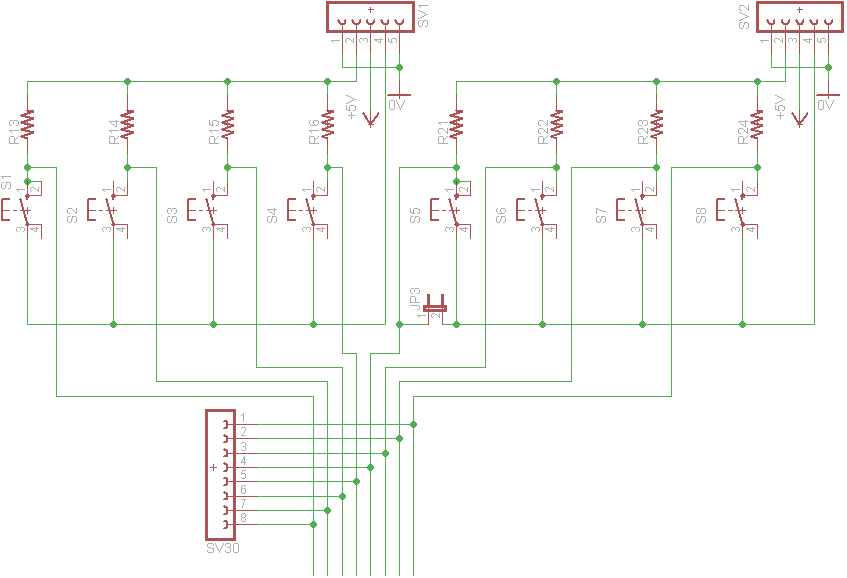
We see the wiring diagram of the section of the digital inputs and focus our attention on streep SV1 and SV2. The configuration is designed so that the same pullup or pulldown resistors may be depending on the jumper is plugged streep all aligned left or right.
The configurations are:
- jumpers left aligned -> Pulldown (logic 1 when the launch button pressed).
- jumpers aligned to the right -> pullup, (i pilsanti throw logic 0 when pressed, normally arrives 1).
The buttons are isolable from the ZIF through the opening of the dip switches, and are withdraw able from the card to be brought where it is necessary, even on the machine using flat cables of the plug-in the corresponding line streep male (for example, SV30 and similar for the other PORT) . Similarly, you can connect the flat cable upstream of the dip switches, or by the side ZIF, giving the ability to enter or exit signals relative to the PORT of PIC. This way I have referred to as "direct I / O".
We therefore maximum flexibility of use.

The photo shows the 16 streep configurable "up / down" divided in groups of 4. In each group of 4 must be engaged at least 2 jumpers, or right-aligned or aligned to the left for failing to pin floating with respect to ground.
In some cases dependent on the type of housing (housing of the controller, or rather box of 40, 28, 18 pins, etc.) the reset button is moved to a different pin number 1. (MCLR is indicated by Baretta denied that the above written or active when the spear to pin logic zero). For this reason it has been inserted the jumper JP3, that in certain cases may also lead simply a power signal to specific pins. The case histories are so many so that the technician uses this system development must make do when you find yourself in front of a particular case. Be aware that due to the great accessibility to the pins, there is always a solution. Please study need some hardware.
Hardware of the ports I / O digital
Inputs
Let's take a quick look, but not too shallow for the operation of ports when configured as digital I / O.

The Pin 2 to 7, excluding the PIN 6, the reference processor are implemented internally in the circuit diagram as shown above. We do a quick analysis:
- Large rectangles: They are Flip / Flop "D" or delay. you get the FF type Set / Reset, in JK variant (which is a particular cascade of SR basics "set / reset"). Is obtained by an FF type D, connecting together the inputs of the JK variant of the SR, but denying via a NOT gate input K with respect to J, and this connection is inside so that, apart from the clock signal, the device presents 3 terminals instead of the canonical 4 more controls than a normal flip flop. The device has the effect of latchare the mark (or keep it in place buffer) adding a kind of delay. The two flip-flop at the top are synchronized with their clock signal, while the lower one, not having this input delays and buffers the signal with respect to what is presented in the form on the TTL input D.
- The outputs Q and Q-denied of these flip-flops are driven by the input signal instead of the two FF type D at the top, these signals correspond to the ignition control or less via PORT = 0b00000001; (referred to RA0), and setting the direction in the TRIS register.
- The P-channel MOSFET is driven when in gate when we are configured as an input and there are no bits outputted via PORT = 0b00000001;
- The N-channel MOSFET has a logic based on when the TRIS register configures the pin as an output, (;) = 0 TRISA and PORTA is driven with all outputs low, ie PORTA = 0b00000000;
- The complementary configuration of the two MOSFETs then determines the output state if set as such or the possibility of reading the bits when input. From here we can expect a moderate current, as already said about 20mmA which is not cheap. We do however take care not to burn sciochette and consequently the door. To give an order of magnitude with this current possimo directly drive an LED with high brightness, or directly drive a seven segment display, or a discrete power transistors.
- Nand the door (with the tip down in the right side of the diagram) is the one that picks up the bits from the field and allows the entrance to the bus and the core of the microcontroller. this is consetito if the signal "analog input mode" is zero, which is derived indirectly from the register Adcon and others. (deepen into suitable location).
- The two flip-flop "latchanno" (which mispronunciation vocabulary) the signals, ie keep the outgoing fixed even if the input signal is no longer present.
- Other circuit elements are of utility intuitive, or invert the signal where it is needed, and simply serve as drivers.

Pin 6 of the processor 16F877 has a configuration Hardware slightly different with respect to pins of the same PORT A, the diagram of which has already been analyzed. In fact to this pin (6 in the reference processor but will have another location in different models) is combined with the "clock signals input to the hardware timer 0" in English "zero timer clock input" abbreviated "T0CKI ".
From this point of view of the architecture of I / O differs from the others for the following things:
- It is combined with an analog channel.
- It works in "open drain", or when set as the output load current through the MOSFET and goes to mass means the only channel "N" available.
- It 'as said combined signal to an external impulse that drives the hardware timer TMR0.
- Structurally it is easier but the more complex features. Sometimes it is better to avoid using this port as well as digital input and output to avoid interface problems or ambiguities programming. All functions are still available.
Outputs
The digital outputs board 24 and are accessible either through "direct I / O" exactly as explained for the inputs, which in free port, eg in the field using portable flat cable plugged in line streep prepared, for example, SV18, SV22, SV23, etc..
In cases where the on-board LED simulation bothered is possible to isolate the line acting in the deep switches S13, on the PORTB, C, D. The signals will be available in Freeport, but the LED will not light.

click on the image above for better view
The DOORS is usually reserved for the control lines of the LCD as it is composed of only three lines and will be explained in the relevant section of the tutorial "Let's go PIC".
Important Note: Although the PORT of PIC are quite robust, arriving at about 20mA, current more than enough these days to drive anything, it is still important to interface with transistor or operational comparators, as well as sections optosolar power.
The PORT B, C, D, E, have all of the additional features or less compared to that base, but in essence work the same way.
At PORT B is combined with such an important function, be enabled by setting the registry ... of the internal pullup, which in some cases allows to exploit the internal mosfet as being a function of the classical 10K resistor which is usually "hang" Vcc to the signal, or to the mass, in order not to have conditions of floating signal before the action button , often normally open (see Micro-GT) placed in series with it.
The most stable configuration, and then by favourite is, as regards the digital inputs is "normal 1 -> command 0" which is obtained for example with a pullup resistor in series with a normally open push button. The signal taken from the center of this series has led directly to the pin as an input configured.

The pins RB0 and RB3 have the internal wiring diagram we see in the picture above. The first thing you notice is the presence of the signal RBPU, as alluded to active low, enables the function of internal pullup (not available nal PORT A). These pullup are automatically turned off when the door is switched to output. The note at the foot of the image makes it clear that there is a recirculation diode and protection, which ensures operation pointed toward Vdd. The presence of the TTL buffer, allows not to burn the point of I / O at the time they arrive at different voltages from 5V, as in the case of programming. (This issue will be thorough, for the moment let us take it so good).
RB0/INT is an input that can acquire an interrupt signal, namely that it launches a service routine for putting a few machine cycles waiting for the current program (the technique of context switching), giving the impression that they are running two simultaneous data from microcontroller to perform tasks. Enabling and configuring the interrupt has this syntax INTDEG bit (OPTION_REG <6>), suggested by the manual of the microchip, in fact we will soon cme done using the C16.
The pins RB6 and RB7 are delegated to the programming circuit.
.jpg)
When using the serial programming mode circuit in low voltage ICSP LVP type and are enabled internal pull-up, log in, reset pin RB3 TRISB.
It 's important to know that the PORT B is not the most suitable operating mode multiplexing due to the presence of its 8-bit extension of these additional features.
And 'more suited to multiplexing and polling on PORT C which carry under the wiring diagram, as in A and B to a single pin.

The PORT C also contains the serial communication ports, and RB3 and RB4 pin can enable the I 2 C communication protocol
We shall see that the RS232C port is connected to pin RX-> TX and RC7 -> RC6.
The PORT E, which has only 3 points of connection, the protocol is designed for PSP, parallel slave port, particularly suitable for communication between two processors, for example between our microcontroller and the on-board LCD display, for example, 2-line for 16 characters, Hitachi second standards.

We'll see when the time like this is connected to PORT AND PORT operation of D with its 8-bit can implement an effective data exchange with peripherals.
- RD -> Active low: RE0
- WR -> Active low: RE1
- CS -> Active low: RE2
The program starts from here
How to create an alias
Quado the program has a certain extension can become complex, or at least awkward to use the canonical name of the points of I / O, for example RA2, RC3, RB0 etc.. for example, by a program in which are mentioned a thousand times and the sequence prescribed by the logic of the program. We see for example the following if statement:
if ((&& RA0 RA1) ^ RA2) {}
If you fill in "main () {}" (the main body is inside the curly brackets) the compilation is successful and creates a. Hex, but frankly it's difficult to read because the variable is anonymous.
The same construct, according to the revised alias looks like this, clearly the most significant:
if ((start && no_allarme) ^ bypass_OK) {}
The program executes the body of 'IF, for example the commencement of an industrial machine, "if" (if = if) (pressed the start command "&&" (and, means "and also"), or within the a consent signal priority, which bypasses the first two conditions, ("or" ^ = logical or)
Considerably more readable!
There remains the problem of how to set these aliases. The syntax is as follows:
# Define RA0 start
We note that the line is not closed with the terminator of ANSI C standard, or ";" this is possbile because the construct "#" (read "number") followed by the construct "define" combines the label (label) to the following point of I / O, d example RA0 ending the command line.

In the image above we see the result of a build platform and compiler Hitech-Lab MP "C16", which is the universal tool suite that is the official instrument of the manufacturer.
I shrunk the windows for reasons of space, but in the top left we have the project tree, bottom left the program running only a minimal alias suk pin RA0 which is named "start", because that is likely to edge machine is the start button, and keep it throughout the program.
In the right column we see the window "sommmario" compilation. We will enter more in future publications of "Let's go PIC". For the moment we mention the fact that shows the areas of memory management, and essential, if the compilation has been successful or not. We see in our example the word *** Build successful! ***, That I wish everyone to see forever or at least as frequently as possible.
-------------------------------------------------- ------------------
Exercise: Create the alias.
Copy the source below and paste it on a notepad file of windows. Save it as "definizione.c" then read the first edition of "Let's go PIC!" and create a project "definizione.mcw". Run the build up to get the file "definizione.hex"
# Include <pic.h>
# Define RA0 start / / implements the alias
void main () {
if ((&& RA0 RA1) ^ RA2) {
}
}
-------------------------------------------------- --------------------
Warning: During the course exercise you encounter problems with file extensions, especially when they create with notepad instead of using the editor built into MP-Hitech Lab. Resolve the issue aditando properties of the folder that contains the file and removing the option in folder properties, hide file extension. If you do not have the impression that this could prova.c a file actually has the dual prova.c.txt hidden extension that will make you go crazy with strange compilation errors and consequent not create the file. Hex to us essential to the flaschare PIC.
Recompile the program by defining RA1 FTC (which indicates a photocell) and RA2 as bypass.
As noted possimo programming using aliases is much more elegant than the one with real addresses, and all in all adds simplicity and readability of the source code. Once you hand you can not do without.
do not read the first, if you failed to successfully complete this exercise.
-------------------------------------------------- --------------------
The debounce software
The mechanical contacts, unlike those in the solid state simulated with transistors or MOSFETs, are Related Subjects to inertia and even worse to elastic reactions that are summarize in "bounces" in the closing phase.
If the reading of this input signal was very rapid, the curve of elongation and subsequent damped oscillations can be interpreted as switching the logic state, thus converting the image the step of heaviside in a comb of rapid pulses capable of generating all instability Automation.
From the electrical point of view it is solved by placing a small capacitor, a few tens of picofard, in parallel to the contact moves into closed. These, having function of low pass filter, short-circuits to ground the high-frequency harmonics of the phenomenon, dulling or eliminating the elongations and the subsequent oscillations of adjustment.
After the transient the capacitor will be charged to the voltage of the logic signal resulting transparent so please. Is introduced uncertainty status during the opening phase, which depend on the speed of discharge of the capacitor, even if the curve being very rapid may resemble strongly to a ramp. There will still never identical to the falling edge of the step in "off" (transition from ON -> OFF logic signal).
The issue of bounce can also be managed by software running on some sort of control "stay high" signal that is presented for a short time but still present after the first detection of the presence.
Ie: I close the contact and I note the presence means the IF construct, but not I agree immediately take effect. I let go I consider to be a time that is necessary to stabilize the bounces, I check if the signal is still present.
If after this sort of "filter" the signal is present, then I let go allowing the effect.
the trick is:
- presence control with IF
- launch of a stabilization time
- rechecking presence with IF
- if the signal is still present I agree the effect executing the body of the second IF.
We see the example and run the second year.
/ ************************************************* *
* Let's GO PIC: *
* September 8, 2010 *
* Capture with debounce "draft" *
* Micro-platform IDE * Versatile PIC GT
* Marco Gottardo *
************************************************** /
# Include <pic.h>
# Include <delay.h>
# Define RA0 button
# Define LED RB0
void main () {
TRISA = 0xFF;
TRISB = 0;
while (1) {
if (button == 1) {
DelayMs (10);
if (button == 1) {
indicator = 1;
}
}
}
}
In the picture we see the environment programming and compiling successful. At
this point you will be very happy and contented because everything is reported,
word for word, the compiler, as a successfully build!, But .... ...
something is wrong. Read the following before you call, as a complement to this exercise, try to think about what I'm trying to tell you is how significant abnormality.

The program is syntactically correct, but has a severe functional defect. If you have read the introductory part, which concerns the 'hardware port I / O will not escape the fact that they are implemented (means performed or constructed) by the Flip / Flop and then there is a memory effect. This memory effect is known as digital electronics "Latch" (translated literally bolt or lock). On the practical side stabilizes output that would be a monostable pulse input.
Test your program with RealPic simulator, taking into account that in the visual you have a button linked to a button at RA0, set up as normal -> 0, pressed -> 1 (the act of setting right on the box tab button ), while the output will put an LED coupled to RB0.
We see the example and run the third year.
/ ************************************************* *
* Let's GO PIC: *
* September 9, 2010 *
* With a debounce Acquisition *
* Micro-platform IDE * Versatile PIC GT
* Marco Gottardo *
************************************************** /
# Include <pic.h>
# Include <delay.h>
# Define RA0 button
# Define LED RB0
void main () {
TRISA = 0xFF; / / set to PORT A all inputs
TRISB = 0; / / set to output all PORT B
while (1) {/ / start the infinite loop
if (button == 1) {/ / test the control condition
DelayMs (10);
if (button == 1) {
indicator = 1, / / turn on output
}
}
if (button == 0) {/ / test the condition denied
DelayMs (10);
if (button == 0) {
indicator = 0; / / off output
}
}
}
}
From below link you can download a zip file containing the libraries delay.he
delay.c the definizione.ce two source files. Hex, the first need to understand
that if you put the command to shut down the opponent or point of I / O The bit
remains latched-ato (what an ugly term, do not use it ever). The second is the
full version of the source or the compiled above. Do this easy exercise, load
the first one and then the other in the simulator "RealPIC simulator" as
explained in the first half of the tutorial, and compared effects.
UserFiles / ad.noctis / definizione.zip
Playing with the outputs
Although in the previous section we have mentioned the digital outputs, as the push of a button connected to the input we turned on the LED connected to RB0, this was very little compared to what a reader expects a little more experienced in the use of digital outputs.
As previously explained, PORT, when configured as outputs through the correct parameterization of the TRIS register, have similar purposes, not identical.
We said that some are more suitable to drive the LCD, others are prepared for certain types of signals, some are open drain, etc.. etc.. strongly depend on the model that we use.
We also said that twenty mill amperes can pull out the drain or in the I / O, Quindio we should not be afraid to directly connect a LED display, though of course we have available ports, and will not be a waste as this will allow us to eliminate the decoder chip, which I preferred not to do in the Micro-GT which mounts on board a BCD decoder 7SEG-type CD4511.
E 'of having to start getting comfortable with the outputs with the classic experiments ... follows the chorus of veterans who still have decided to read .... NOOOOOOO! SUPERCAR NOOO!!
But what can I do? is a must, and indeed also in great demand and especially by the popular boys in the age group I teach at school.
Let's do this .... I homeschool for many years even in business education, so even people who are already out of college, content with their first, and then make my boys happy with the many field SUPERCAR.
Exercise number 4.
The Micro-GT, a built-BCD decoder 7segmenti LED driven by the CD4511 chip. This IC accepts 4 input lines of the BCD code and decode the combinations necessary to turn the display segments in a corresponding manner, for example here is that if he presented the 0011 combination will set its output lines in a manner consistent power the number 3, if we propose the combination 0100 he decodes the 7 lines that turn a combination number 4, and so on for the digits 0 to 9. The other 6 combinations available, in fact 2 4 = 16, as expected from the algebra combinatorial, are called redundant, that is meaningless. Experts can use these combinations to send in a shared bus control signals or information "encrypted". or rather transparent to the display that will let no light.
Click on the link for the technical documentation of the integrated CD4511.
The exercise I propose is quite simple, but highly application. In fact, my philosophy is basic simplicity above all in the learning phase. Not deny that these little programs are an expert on the threshold of ridicule, but as they say in my part, in the Veneto, Nobody is born learned ... ME FIRST.

wiring diagram of the 7-segment display section of the GT-PIC Micro versatile IDE
The diagram speaks very clearly, the 4 displays are common cathode which is connected mass, allowing the current to turn on the same segment through an "electronic switch", made with a type BJT BC337, classic transistor for signal , NPN as shown in the diagram. The resistors R8, R9, R10, R11, limit the RB to the value sufficient to saturate to the component. In this condition the voltage drop between the collector and emitter is close to zero (except for a small residue of approximately 0.2 V) and behaves accordingly as a switch. Upstream of the base resistances are the 4 CONNECTIONS available in either Freeport or linking to the PORT we want via a flat cable, or simply closing the deepswitch accepting your connection to the bus PORT I chose in the design phase, and vincoladovi software to drive that specific PORT. (see wiring diagrams)
If we use the bus by default connect the ignition of the display takes place only enabling the bus lines acting on the deep SV26.
The control lines, or the bases of the transistors, and the line data that go to the BCD decoder / 7 segments are separated on two furture streep line males shown in screen printing with SV19 (data line) and SV20 (line control mode).
Also, the decimal points, if we were interested to turn them on are available in Freeport mode, then using flat cable and close the streets in S25 deep interest.
Important Note: If you develop a demoboard with the pattern that I have provided you remember to connect masses above the mass of your mainboard, or one where you have the processor, otherwise it will not turn on anything.
The affected section is located in the area indicated by the pink rectangle in the picture of PIC Micro-GT shown below.

section of the 7-segment display of the Micro-GT Versatile PIC IDE
Text of the year.
At the push of a button we turn to display the corresponding number, eg 1 key on the display 1, 2 key on the display 2, etc..
Solution
/ ************************************************* *********************
* Let's GO PIC! September 9, 2010 *
* Marco Gottardo *
* MICRO-GT versatile IDE PIC *
* Program dialing *
* No matching key number to display that displays the number n * n
************************************************** ******************** /
/ / Sets the frequency of the quartz
# Define XTAL_FREQ 20MHz
# Include <pic.h>
/ / Merged configuration
__CONFIG (HS & WDTDIS & PWRTEN & BORDIS & LVPDIS & DUNPROT & WRTEN & DEBUGDIS &
Unprotect);
# Include <delay.h>
# Include "setting.h"
/ / Test program interrupt
void main (void) {
settings ();
while (1) {
if (P1 == 0) {
DelayMs (10) ;/ / delay
if (P1 == 0) {
PORTC = disp1;
PORTB = 1;
}
}
if (P2 == 0) {
DelayMs (10) ;/ / delay
if (P2 == 0) {
PORTC = disp2;
PORTB = 2;
}
}
if (P3 == 0) {
DelayMs (10) ;/ / delay
if (P3 == 0) {
PORTC = disp3;
PORTB = 4;
}
}
if (P4 == 0) {
DelayMs (10) ;/ / delay
if (P4 == 0) {
PORTC = disp4;
PORTB = 8;
}
}
}
}
This program contains many points of discussion. For example, the line of code:
__CONFIG (HS & WDTDIS & PWRTEN & BORDIS & LVPDIS & DUNPROT & WRTEN & DEBUGDIS & Unprotect);
We met for the first time. This sets the log of the FUSE settings that are essential for the proper functioning of the PIC. The line begins with two "underscore" that combines the editor giving the impression that one, then everyone of helminths separated by "&" correspond to a BIT that enables or disables a feature, let's call system.
see for example the first two: HS and WDTDIS. are respectively the setting hardware interior so that it can accept a external crystal at high speed, High speed, and the "DIS" or disabling the "WDT" famous watchdog timer. Give only a brief mention of the fact that this timer is reset automatically whenever the program counter goes through the first line of code. If the timer expires before a subsequent restart means that the processor and then the program has crashed, and then no longer able to respond to the stresses or stimili on its endings I / O. In this case the intervention of the WDT freezes the whole system to avoid the serious Davvi that automation can do when it is deprived of "control".
The register of FUSE, their study and use deserve a separate section of our tutorial "Let's go PIC". Just have a free moment I work a little.
If this line is not inserted in the source code then you can set the merged directly from the software development.
menu 'configuration' of MP-Lab call 'configuration bits'. appears in the following box settings.

Now let's a question: Why set the fuse on the code as lopossiamo externly do software development?
Answer: There is a software that allows the strategy insertion microcode, or
dell'hex inside the PIC without using its software programming and development
(such as MP-Lab), a development board, but it simply card " target "which of
course put at least at the disposal of the doors communication.
This mode flachare the PIC does not even require the high voltage (13.2 V i that provides the Micro-GT) because everything happens in low power mode, the one that is already available to power the PIC, we look for example The fifth item on the image "configuration bits" above.
I will devote a chapter of the tutorial programming via bootloader. for moemnto is better not to deviate too much from that are the focus article digital I / O.
When the code becomes very articulate it well to exploit the capacity of "C" to be divided into external modules then linked into a single file before being assembled.
The # include directive is used only for library files for any external modules of our program, they both header "header" saved as. H, or actual sources of the methods and content stored functions. C
In the programming philosophy of "C" header files (. H) contains prototypes and definitions of any commands library.
Here is the source of the external module setting.h
-------------------------------------------------- --------------------------------------------
/ / Basic program developed for 16F877A
/ / Close the channels of the DIP SW1 5 to 8
/ / Open the channels of the DIP SW1 1 to 4
/ / Connect with the 4-wire flat cable chick with SW22 SW19
/ / Inputs of the CD4511 decoder correspond to:
/ / A -> RC0
/ / B -> RC1
/ / C -> RC2
/ / D -> RC3
A RC0 # define / / -> pin 15
RC1 # define B / / -> pin 16
# Define C RC2 / / -> pin 17
# Define D RC3 / / -> pin 18
# Define digit4 RB0 / / pin 33 (LSB) on the right most digit
# Define digit1 RB1 / / pin 34
# Define DS2 RB2 / / pin 35
# Define DS3 RB3 / / pin 36 (MSB) on the left most digit
/ / 1 = normal buttons, pressed = 0
/ / Use 10K ohm pull-up
/ / SV2 jumper with right-aligned
/ / The GATE input is switched
# Define P1 RA0 / / write commands (1) of digit 1
# Define P2 RA1 / / write commands (2) of digit 2
RA2 # define P3 / / write commands (3) of digit 3
RA3 # define P4 / / write command (4) digits of 4
disp1 char = 1, / / used in the function module in scriviBUS writeBUS
disp2 char = 2;
char disp3 = 3;
disp4 char = 4;
void settings (void) {
TRISA = 0xFF;
TRISB = 0;
TRISC = 0;
TRISD = 0;
TRISE = 0;
}
-------------------------------------------------- -----------------------------------
From this link you can download the solution of this exercise:
UserFiles / ad.noctis / select_number (11). Zip
Second version:
We want to perform an automatic display of the numbers to diplay. Each digit is multiplexed
/ *************************************************
******************************
* MICRO-GT versatile IDE PIC *
* Program dialing *
* Version of both automatic and manual *
* No matching key number to display that displays the number n * n
* In the automatic mode by pressing the number P5 generates 1Hz *
************************************************** *****************************
/
/ / Sets the frequency of the quartz
# Define XTAL_FREQ 20MHz
# Include <pic.h>
/ / Merged configuration
__CONFIG (HS & WDTDIS & PWRTEN & BORDIS & LVPDIS & DUNPROT & WRTEN & DEBUGDIS &
Unprotect);
# Include <delay.h>
# Include "setting.h"
void main (void) {
settings ();
while (1) {
if (P1 == 0) {
DelayMs (10) ;/ / delay
if (P1 == 0) {
PORTC = disp1;
PORTB = 1;
}
}
if (P2 == 0) {
DelayMs (10) ;/ / delay
if (P2 == 0) {
PORTC = disp2;
PORTB = 2;
}
}
if (P3 == 0) {
DelayMs (10) ;/ / delay
if (P3 == 0) {
PORTC = disp3;
PORTB = 4;
}
}
if (P4 == 0) {
DelayMs (10) ;/ / delay
if (P4 == 0) {
PORTC = disp4;
PORTB = 8;
}
}
if (P5 == 0) {
DelayMs (10) ;/ / delay
while (P5 == 0) {
/ / If (P5 == 0) {
PORTC = disp1;
PORTB = 1;
DelayMs (200);
PORTC = disp2;
PORTB = 2;
DelayMs (200);
PORTC = disp3;
PORTB = 4;
DelayMs (200);
PORTC = disp4;
PORTB = 8;
DelayMs (200);
/ /}
}
}
}
}
-------------------------------------------------- -----------------
The next source is the setting.h, unique to this automatic version and the Micro-GT PIC. to turn on the display have to do correctly so that the signals traveling correctly along buses enable the deepswitch and setting the appropriate jumpers.
To be done is indicated as a comment, or after the double Slach "/ /" on the front lines and setting file. H you see below.
Please leave these comment lines within the file. will be very useful.
-------------------------------------------------- ------------------
/ / Basic program developed for 16F877A
/ / Close the channels of the DIP SW1 5 to 8
/ / Open the channels of the DIP SW1 1 to 4
/ / Connect with the 4-wire flat cable chick with SW22 SW19
/ / Inputs of the CD4511 decoder correspond to:
/ / A -> RC0
/ / B -> RC1
/ / C -> RC2
/ / D -> RC3
A RC0 # define / / -> pin 15
RC1 # define B / / -> pin 16
# Define C RC2 / / -> pin 17
# Define D RC3 / / -> pin 18
# Define digit4 RB0 / / pin 33 (LSB) on the right most digit
# Define digit1 RB1 / / pin 34
# Define DS2 RB2 / / pin 35
# Define DS3 RB3 / / pin 36 (MSB) on the left most digit
/ / 1 = normal buttons, pressed = 0
/ / Use 10K ohm pull-up
/ / SV2 jumper with right-aligned
/ / The GATE input is switched
# Define P1 RA0 / / write commands (1) of digit 1
# Define P2 RA1 / / write commands (2) of digit 2
RA2 # define P3 / / write commands (3) of digit 3
RA3 # define P4 / / write command (4) digits of 4
# Define P5 RA4 / / cycle loop controls of digits 1-2-3-4
disp1 char = 1, / / used in the function module in scriviBUS writeBUS
disp2 char = 2;
char disp3 = 3;
disp4 char = 4;
void settings (void) {
TRISA = 0xFF;
TRISB = 0;
TRISC = 0;
TRISD = 0;
TRISE = 0;
}
-------------------------------------------------- ----
This program includes a second header file and name it writebus.h whose source code is below. It contains only the function of writing to the port and thus the ivio data to the decoder CD4511 of the development board.
-------------------------------------------------- ------
void scriviBUS () {
if (PORTB == 0b0001) {
}
if (PORTB == 0b0010) {
}
if (PORTB == 0b0100) {
}
if (PORTB == 0b1000) {
}
PORTC = disp1;
}
-------------------------------------------------- ----
Ultimately, the automatic version of the scripture, Thou shalt numbers on dislay 7-segment consists of three files:
- writeBUS.h
- select_number_auto.c
- setting.h
to which I add the fourth, the file:
select_number_auto.hex
that you will find the zipped file here for download here:
UserFiles / ad.noctis / select_number_auto.zip

In the picture of a particular terminal for connection of the stepper motor sits above the display includes seven segments used in these exercises.
Appendix:
Effect lights supercar: The hello world of those who started with the PIC
As promised I will now try to please beginners with some variant of the classic exercise "supercar". Those already experienced will jump at the bottom of this section, also because, as we well know, the programming routines delay line is wrong in concept, since the processor is put on hold the end of a time and in the meantime is not paying attention what happens in its periphery. We mention, but will investigate a after chapter and in ordinary things of the processor must be "broken" by his task to back them with a technique called priority interrupt.
I think that a beginner can certainly grasp the concept but do not think it can develop a program or even just for a gestirene already.
Let's go step by step and then once acquired the necessary experience will all be faced with greater equanimity.
Supercar program for beginners:
16F877A microcontroller, system development Micro-GT Versatile PIC IDE
Select the clock at 20MHz with jumpers (see diagrams).
Enable PORTB PORTC and the acting on the corresponding deepswitch.
Set as generally mounted buttons open, or normal -> 0, pressed -> 1. If you realize the real system will then "normally open switches with resistive pulldown.
If you use lamps with power sure to drive the triac with the appropriate optocouplers.
Download the hex file that I made available and test it with Realpic simulator (see the first part of let's go pic for more detailed explanation.
Given the didactic nature of this simple program I do not assume any responsibility for its possible use outside of this area, I also clearly said sixth of the programming method with routine delay inline concept is wrong. Similar programs are developed with the technique of the interrupt.
Here's the source code:
/ ************************************************* ************************
* Let's GO PIC: managing digital I / O *
* Micro-GT developed for versatile IDE PIC *
* September 13, 2010: Marco Gottardo *
* Correctly set the jumpers on demoboard *
* The inputs are bistable (NA switches) *
**
* Available effects: *
* Car1 -> effect supercar PORT B *
CHAR2 * -> C * PORT to effect Superca
* Car1_2 -> Superca effect continues on the PORTB PORTC *
**
************************************************** *********************** /
# Include <pic.h>
# Include <delay.h>
RA0 # define car1
# Define CHAR2 RA1
# Define car1_2 RA2
# Define stop RA3
void main () {
TRISA = 0x3F, / / 6 bits of Port A configured as inputs
TRISB = 0; / / the entire output port B
TRISC = 0; / / the entire output port C
PORTB = 0b00000000; / / initialize port B all off
PORTC = 0b00000000; / / initialize port C all off
while (1) {
if (car1 == 1) {/ / PORT B to effect supercar
PORTC = 0b00000000; / / reset the port not in use
PORTB = 0b00000001;
DelayMs (255);
PORTB = 0b00000010;
DelayMs (255);
PORTB = 0b00000100;
DelayMs (255);
PORTB = 0b00001000;
DelayMs (255);
PORTB = 0b00010000;
DelayMs (255);
PORTB = 0b00100000;
DelayMs (255);
PORTB = 0b01000000;
DelayMs (255);
PORTB = 0b10000000;
DelayMs (255);
PORTB = 0b01000000;
DelayMs (255);
PORTB = 0b00100000;
DelayMs (255);
PORTB = 0b00010000;
DelayMs (255);
PORTB = 0b00001000;
DelayMs (255);
PORTB = 0b00000100;
DelayMs (255);
PORTB = 0b00000010;
DelayMs (255);
}
if (CHAR2 == 1) {/ / PORT C to effect supercar
PORTB = 0b00000000; / / reset the port not in use
PORTC = 0b00000001;
DelayMs (255);
PORTC = 0b00000010;
DelayMs (255);
PORTC = 0b00000100;
DelayMs (255);
PORTC = 0b00001000;
DelayMs (255);
PORTC = 0b00010000;
DelayMs (255);
PORTC = 0b00100000;
DelayMs (255);
PORTC = 0b01000000;
DelayMs (255);
PORTC = 0b10000000;
DelayMs (255);
PORTC = 0b01000000;
DelayMs (255);
PORTC = 0b00100000;
DelayMs (255);
PORTC = 0b00010000;
DelayMs (255);
PORTC = 0b00001000;
DelayMs (255);
PORTC = 0b00000100;
DelayMs (255);
PORTC = 0b00000010;
DelayMs (255);
}
if (car1_2 == 1) {/ / PORT B effects from long-continued on PORTC
PORTB = 0b00000001;
DelayMs (255);
PORTB = 0b00000010;
DelayMs (255);
PORTB = 0b00000100;
DelayMs (255);
PORTB = 0b00001000;
DelayMs (255);
PORTB = 0b00010000;
DelayMs (255);
PORTB = 0b00100000;
DelayMs (255);
PORTB = 0b01000000;
DelayMs (255);
PORTB = 0b10000000;
DelayMs (255);
PORTB = 0b00000000; / / clears PORTB to continue on C
PORTC = 0b00000001;
DelayMs (255);
PORTC = 0b00000010;
DelayMs (255);
PORTC = 0b00000100;
DelayMs (255);
PORTC = 0b00001000;
DelayMs (255);
PORTC = 0b00010000;
DelayMs (255);
PORTC = 0b00100000;
DelayMs (255);
PORTC = 0b01000000;
DelayMs (255);
PORTC = 0b10000000;
DelayMs (255);
PORTC = 0b01000000;
DelayMs (255);
PORTC = 0b00100000;
DelayMs (255);
PORTC = 0b00010000;
DelayMs (255);
PORTC = 0b00001000;
DelayMs (255);
PORTC = 0b00000100;
DelayMs (255);
PORTC = 0b00000010;
DelayMs (255);
PORTC = 0b00000001;
DelayMs (255);
PORTC = 0b00000000 ;/ / clears the memory effect PORTC
PORTB = 0b10000000;
DelayMs (255);
PORTB = 0b01000000;
DelayMs (255);
PORTB = 0b00100000;
DelayMs (255);
PORTB = 0b00010000;
DelayMs (255);
PORTB = 0b00001000;
DelayMs (255);
PORTB = 0b00000100;
DelayMs (255);
PORTB = 0b00000010;
DelayMs (255);
PORTB = 0b00000001;
DelayMs (255);
}
if (car1 == 0) {
PORTB = 0b00000000; / / clears memory, turned off all port B
}
if (CHAR2 == 0) {
PORTC = 0b00000000; / / clears memory, turned off all port C
}
}
}
download the complete program from this link with the file. hex to try and flaschare simulator on the PIC.
It also contains libraries delay.he delay.c to copy the include directory EDL compiler.